Using an LDO vs. Switching Regulator in Your PCB
As much as we’d like, the power we supply to electronics isn’t always stable. Real power sources contain noise, they might exhibit power instability, or they dropout unexpectedly. Thankfully, we have power regulators to help prevent some of these problems.
For low power devices, we generally see two types of power regulators: a low dropout regulator (LDO) or a switching regulator. You can mix and match these at different points along your power bus, but there’s still the matter of choosing whether to use an LDO vs. a switching regulator in your designs.
If you’ve ever wondered how these decisions are made and when to use each type of regulator, just know that there is more to this decision than simply looking at the input/output voltage/current. Keep reading to learn more about selecting an LDO vs. a switching regulator for your low power designs. Since we’re interested in PCB layout on this blog, I’ll briefly discuss what needs to happen in the layout to support an LDO or switching regulator.
LDO vs. Switching Regulator Comparison
Before getting into component arrangement and layout with these types of power regulators, it’s best to get a reminder of how each of these circuits work. An LDO is a step-down linear DC-DC voltage converter, so it’s best compared to a buck converter. There are also resistive linear regulators, or series and shunt regulators that use transistors, but I’ll leave these alone for the moment as they are not often used on the power bus in a PCB.
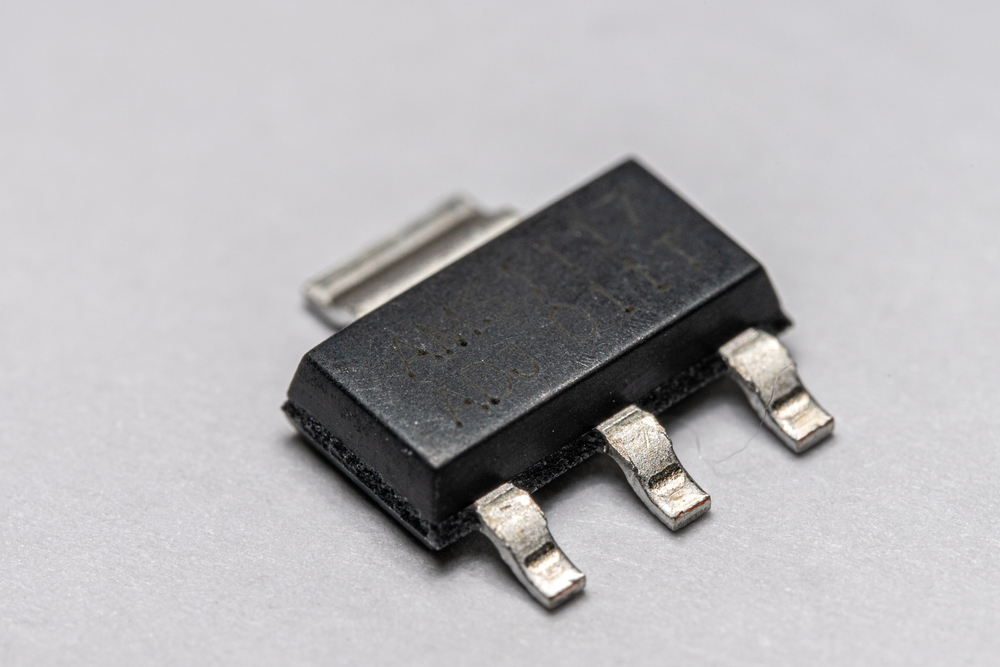
Low Dropout Regulator (LDO)
An LDO is a linear regulator that is based on an op-amp. The circuit operates by comparing the regulator output and a reference voltage (silicon bandgap reference with ~1.25 V output) within a feedback loop. The basic topology is shown below. Note that an NPN transistor is used in this diagram, but you’ll normally find a MOSFET in real circuits.
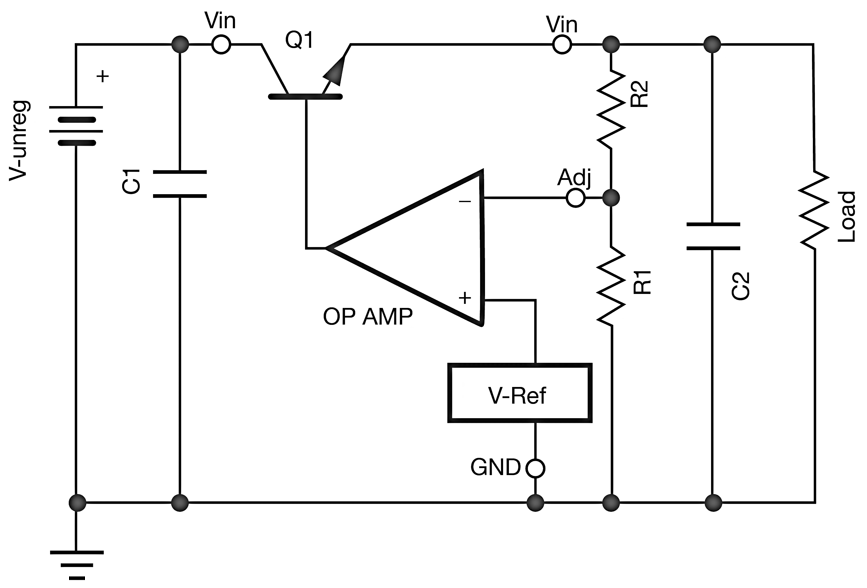
Headroom in an LDO
An LDO has some “headroom,” also known as the dropout voltage, which is a small voltage above the nominal output that determines whether the component will turn on. As long as V(in) - V(out) > Headroom, then the component will give the nominal output voltage. The voltage divider is used to drop down the input voltage so that the op-amp can compare it with the reference voltage (V-Ref). Unless you’re building an LDO from discrete components, you won’t need to worry about setting up an op-amp circuit and selecting R1/R2; these are integrated into the component.
Finally, C1 and C2 are filter capacitors that clean up the voltages on the input and output, respectively. These values will not affect the headroom, although they will help dampen noise on the input and output. The op-amp sets the regulator’s output to a desired level as long as the input voltage is above the headroom for the regulator.
Buck Converter
As was mentioned above, an LDO is best compared to a buck converter as they are both step-down components. The goal of any switching converter is simple: to produce a stable, yet adjustable, output voltage by modulating the current and voltage delivered to a load with a switching element. This is normally a power MOSFET driven with a PWM signal, although a much larger regulator like a resonant LLC converter may use multiple MOSFETs in parallel to provide high current output. In any case, all buck regulators will suppress low frequency variations in the input voltage, but the output will have some high frequency noise due to the switching action of the MOSFET, which can be clearly seen in a simulation.
Comparison
So when should you use each of these regulators? They both step down a DC voltage to a useful level while cleaning up noise, so shouldn’t they be interchangeable? Actually, they are sometimes interchangeable, but it depends on the power level you need and the characteristics of the power source. The table below summarizes some of the different aspects of each type of these circuits and their advantages.
|
|
|
|
|
|
|
|
|
|
|
|
|
|
|
|
|
|
|
|
|
|
|
|
|
|
|
|
There is a lot going on in this table, but I’ll do my best to summarize a few points here.
- LDOs are low-noise alternatives to switching regulators. They are simpler to layout and tend to cost less.
- LDOs are sometimes used downstream from a switching regulator to further step down the voltage to a low level. In fact, some switching regulator components include an LDO on the output; see ADP5037 for an example.
- Switching regulators can provide very precise voltage control that only requires adjusting the PWM driving frequency. In an LDO, control is passive.
PCB Layout for LDOs and Switching Regulators
This is a rather in-depth topic in that the PCB layout portion can focus on the regulator circuit, the power bus, and the downstream loads. There are two guidelines I prefer to follow:
- Pay attention to trace width required to support your desired current, keep IR drop low, and keep temperature within safe limits. Don’t be afraid to use polygon pour when you’re working at high current.
- Keep loop inductances small. This means keep components close to each other and trace out return paths in the PCB to ensure you’re not creating an EMI problem.
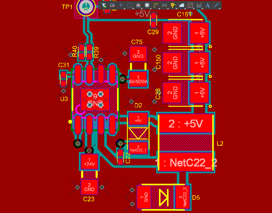
The image below should illustrate what I mean. This layout is for a switching regulator operating at 3 MHz. You’ll notice that the critical portion, namely the loop created by L2 and the filter caps, has a tight circular return path back to the nearby ground pour. This helps ensure low radiated EMI emission and reception. The same principles would apply to an LDO, although in that case we worry more about reception of EMI as there is no switching.
You’ll often see layout examples in application notes for LDOs or switching converters. Be careful with these; they may be just fine for handing the current, but there may be an EMI problem lurking in their layout. These EMI problems in application notes often originate from poorly defined return paths or failure to create a compact layout with low loop inductances. Mark Harris shows a great example of a compact PCB layout for a switching regulator in a recent article, take a look to see some good guidelines from an experienced layout engineer.
Ove you’ve decided between an LDO vs. switching regulator in your PCB layout, use the best set of CAD tools and component management features in Altium Designer® to place and route your designs. When you’ve finished your design, and you want to release files to your manufacturer, the Altium 365™ platform makes it easy to collaborate and share your projects. We have only scratched the surface of what is possible to do with Altium Designer on Altium 365. You can check the product page for a more in-depth feature description or one of the On-Demand Webinars.
