Switched-Mode Power Supply PCB Layout Guidelines
Power supply designers understand the complex technical details and functional requirements involved with a switched mode power supply PCB layout. The layout determines susceptibility to electromagnetic interference (EMI), thermal behavior, power integrity, and safety. A good layout ensures high efficiency power conversion and delivery to a load while allowing heat transport away from hot components in the layout, and it ensures low noise coupling around an electronic system. Safety is also an important factor in switching regulators, which might source high current to an output, creating a safety hazard.
Poor layout choices introduce problems that occur at high current levels and become obvious with large differences between input to output voltages. Common power supply problems seen with a bad PCB layout include loss of regulation at high output current, excessive noise on the output and switching waveforms, and circuit instability. With a combination of DC power integrity simulation tools, circuit simulation and analysis features, and the best set of layout and routing utilities, designers can ensure their device will be safe and reliable. Altium Designer offers power supply PCB layout software and much more that helps prevent these problems.
ALTIUM DESIGNER
PCB design software that helps you follow switched-mode power supply PCB layout guidelines.
Power supplies face a range of challenges and require a complete set of design and analysis features to ensure they operate properly. These designs can also create safety hazards that can hard users, both through exposure to high voltage and a sudden discharge of current into the user. How can designers make sure they can build safe, accurate, and reliably power supplies?
Switched-mode power supplies are standard for converting between high-current rectified AC and high-voltage through the use of a switching power element in a reactive circuit. These components are nonlinear and often use feedback to maintain regulation, in contrast to the typical LDO regulator. In an LDO, regulation is maintained through saturation of an error amplifier, creating resistive losses that are seen as heat in the PCB layout.
While switching regulators are preferred from a regulation and efficiency standpoint, they can be difficult to lay out as they involve more components, some of which will have larger parasitics and can be susceptible to noise problems if not arranged properly. To get started with your next power supply layout, follow these switched-mode power supply PCB layout guidelines so you can ensure your design is reliable.
Starting Your SMPS PCB Layout
There are some basic SMPS PCB layout rule to follow that will help ensure your design has low noise problems, low radiated EMI, and stays at low temperature. Broadly, these guidelines can be summarized as follows:
- Try to keep EMI low by properly defining ground, placing short routes in the PCB layout, and arranging galvanically isolated sections in the PCB such that there is no noise coupling.
- Make use of appropriate input and output EMI filter circuits when needed if there is noise in the layout, features like envelope tracking are needed, or specific noise sources are causing problems in the design.
- Use plenty of copper to provide a path for heat dissipation away from important components. If needed, you might consider a unique enclosure design, as well as heat sinks or fans on hot components.
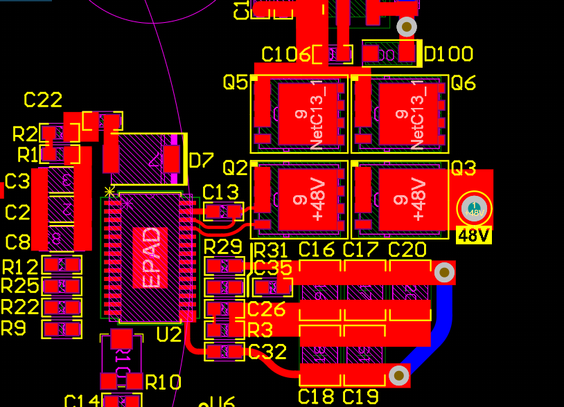
- Place fast switching, high-current circuits like MOSFET arrays so that there are no parasitic oscillations in the design during switching events.
Regulatory bodies such as Underwriter Laboratories and the IEC test power supplies for radiated electromagnetic interference (EMI), conducted EMI, stability, efficiency, and operating life. FCC and CE regulations also set limits on emissions from switched-mode power supplies as these devices can be unintentional radiators. Altium Designer provides the circuit analysis tools you need to learn more about your device's electrical behavior, and the PCB layout tools can help you create a layout that satisfies the above requirements while considering your simulated electrical specifications.
Be Careful When Defining Ground
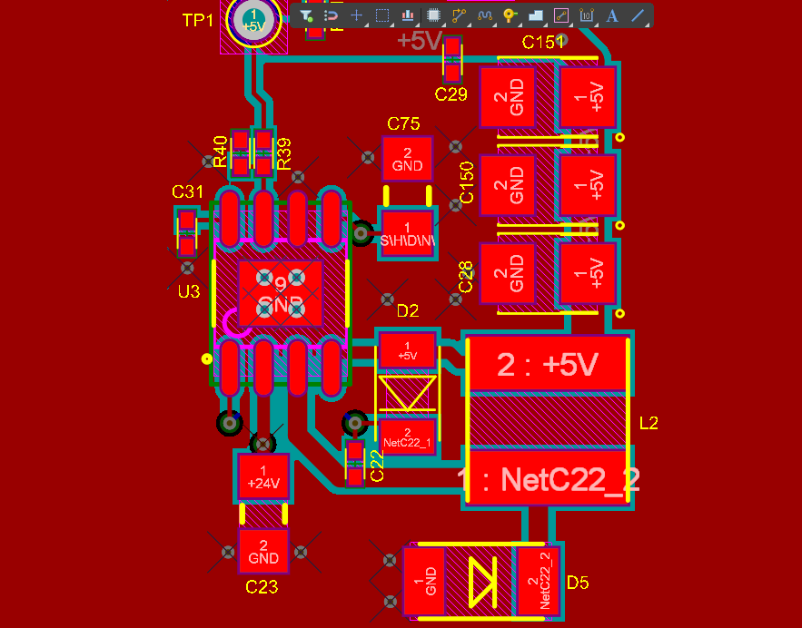
The first switched-mode power supply PCB layout guideline to consider is how to define ground in the layout. As you design your switching power supply circuit, remember that five ground points exist. These may be separated into different conductors to ensure galvanic isolation. These are:
- Input high-current source ground
- Input high-current current loop ground
- Output high-current rectifier ground
- Output high-current load ground
- Low-level control ground
Each of these ground connections might exist in physically separate conductors, depending on the need for galvanic isolation in the converter, rectifier, or regulator circuit. Your power supply circuit can admit common-mode noise if grounds are coupled capacitively, such as can commonly occur through a nearby conductive enclosure. Ground regions in a PCB should be clearly defined on each side of isolating components, such as
If, for some reason, grounds do need to be bridged to eliminate some DC offset, a Y-rated capacitor is the best option as this provides high-frequency filtering and eliminates DC offset between ground regions.
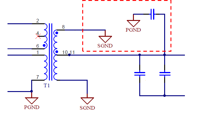
Each high-current ground serves as one leg of current loops, but it should be laid out to provide a low-impedance return path for currents. This might require multiple vias back to the ground plane to admit high current with low equivalent inductance. These points and the potential at which they sit with respect to a system ground become the point for measuring the DC and AC signals that conduct between different points of the circuit. Because of the need to prevent noise from the high-current AC grounds escaping, the negative terminal of the appropriate filter capacitor serves as the connecting point for the high-current grounds.
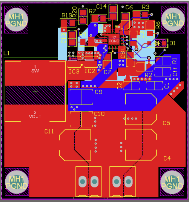
The best practice for defining ground regions is to use large planes or polygon pour. These regions provide low-impedance paths to dissipate noise away from the DC output, and they can handle high return currents .They also provide a path for heat transport away from important components when needed. Placing a ground plane on both sides absorbs radiated EMI, reduces noise, and decreases ground loop errors. While working as electrostatic shields and dissipating radiated EMI within eddy currents, ground planes also separate the power traces and components of the power plane from the signal plane components. Altium Designer's CAD tools make it easy to define grounds in your PCB layout and place large conductors to use as ground regions in your PCB. Especially when working with switching power supplies, you can use a ground plane on both sides of the PCB and bridge them with vias to ensure consistent potential across your grounds.
- Ground regions in a design can be given multiple names depending on their function. Take care when defining ground regions in your design and make sure to link them together properly.
Learn more about earth, digital and analog grounding for circuit boards. - Ground planes are important in systems beyond power supply PCB layouts. Make sure you define connections to have low impedance without affecting assembly.
Learn more about creating a ground plane within Altium Designer. - Common-mode noise and conducted ripple are the dominant noise sources in a PCB layout and they can cause a design to fail EMI testing when noise is extreme.
Learn more about EMI in power supplies and some steps to reduce it.
Schematic Editor Assists Layout
Grounding is an important place to start the design as it will determine the noise immunity and routability of the PCB layout. However, it is not the only consideration in power supply design. Switching action and EMI suppression are built into power supplies and need to be clearly defined in the PCB.
Where to Make Ground Connections
The ability of the SMPS controller to precisely regulate the output voltage depends on the connection of the low-level control ground. As you work with integrated circuits, input capacitors, output capacitors, and output diodes, ensure that the components connect to a ground plane. The ground connection ties to a point where the control IC and its associated circuitry measure the AC current, DC current, the output voltage, and other major parameters. Connecting the low-level ground to the lower side of the current sensing resistor or the output voltage divider prevents the control circuit from sensing common mode noise.
Designing Switching Action
An SMPS operates by rapidly switching the pass units between the cutoff operating state and the saturation operating state and delivering constant power to an output load. At cutoff, high voltage exists across the pass unit but no current flows. At saturation, high current flows through the pass unit with a very small voltage drop. Because the semiconductor switch creates an AC voltage from the DC input voltage, the SMPS can either step up or step down the voltage with transformers and then filter the voltage back to DC at the output.
Pulse-width modulated (PWM) switching power supplies operate either in forward-mode or boost mode. Forward-mode supplies have an L-C filter at the output that creates a DC output voltage from the volt-time average of the output obtained from the filter. To control the volt-time average of the signal, the switching power supply controller changes the duty cycle of the input rectangular voltage.
Buck Converter vs. Boost Converter
Boost converter mode supplies connect an inductor directly across the input voltage source when the power switch turns on. The inductor current increases from zero and reaches its peak simultaneously with turning off the power switch. An output rectifier clamps the inductor output voltage and prevents the voltage from exceeding the supply output voltage. When energy stored in the core of the inductor passes to the output capacitor, the switched terminal of the inductor falls back to the level of the input voltage.
Meanwhile, buck converter mode supplies use the same components, but in a different topology to clamp the inductor's back EMF at a lower level than the input voltage. Switching action provides the same effect as in a boost converter, where the output current oscillates in competition with a charging/discharging capacitor, thus enabling regulation of the output power. Both types of regulator/converter topologies will allow switching noise to propagate to the output ports in the design, which can be seen as a high frequency ripple on the output.
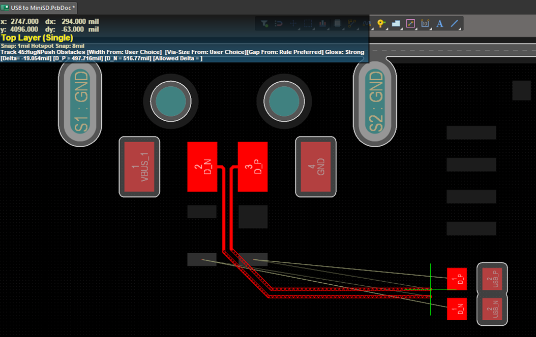
Power Supply Routing Helps Ensure Low-Noise Operation
Switching power supplies conduct high-frequency noise until the noise frequency reaches approximately 100 times the switching frequency. Then, the noise frequency falls at a rate of -20 to -40 dB per decade. Because switching regulators operate with “on” and “off” power states, large current pulses with sharp edges flow within the switching power supply circuit and—as a result—create EMI. The transition between ON and OFF power states creates EMI, which can be induced elsewhere in your system if current loops in the power supply layout are too large. Switching power supply circuits consist of a power switch loop and output rectifier loops, and these need to be routed properly to prevent excessive noise.
When laying out the power supply, pay specific attention to the circumference of the loops and the length and width of traces. Keeping the loop circumference small eliminates the possibility of the loop working as a low-frequency noise antenna. From the perspective of circuit efficiency, wider traces also provide additional heat sinking for power switches and rectifiers. You can use the active route routing engine to achieve human routing results and arrange your components to allow the switching current loops to conduct in the same direction. With the current loops conducting in the same direction, the control circuitry couples to specific spots in the layout. As a result, the magnetic field cannot reverse along the traces located between the two half-cycles and generate radiated EMI.
- Altium Designer's routing tools help you easily place polygons for high current/high voltage lines, or thinner traces for data and control lines.
Learn more about routing your power supply layout in Altium Designer. - When working with the power supply layout, keep traces that handle high switching currents short, direct, and thick. IPC standards can be used to calculate recommend trace widths, although a rule of thumb is a minimum width of 15 mils per Ampere.
Learn more about calculating trace width to ensure high current carrying capacity. - EMI filters within the SMPS suppress high-frequency noise caused by the high-frequency currents conducted within the DC input and output wiring. You can use the integrated component pricing and availability and the datasheet links found within Libraries and the Altium Content Vault to design filters that give the best results.
Learn more about EMI filter circuits in your PCB layout.
PCB Layout Tips for SMPS AC Voltage Nodes
Depending on the SMPS configuration, the AC voltage nodes exist at the drain of the power MOSFET or the collector of a BJT and the anodes of the output rectifiers. Each of these nodes can have high AC voltages. As an example, the peak-to-peak AC voltage found at the MOSFET drain can measure one to two times the input voltage. With the drain bolted to a heatsink through an insulator, the earth-grounded heat sink provides a path for capacitively coupled noise. You can use the PCB layout tools found in Altium Designer to place susceptible signals on the same side rather than underneath a noisy AC node. In addition, you can cross-hatch any ground planes located under the node to eliminate the noise.
Surface mount environments have smaller values of capacitance but can couple noise into sensitive signals. Because of those factors, your layout also needs to address the possibility of capacitive coupling of the AC node voltages into heat sinks or adjacent ground planes. When laying out a surface mount PCB design, make the nodes large enough to serve as heat sinks for either the power switch or rectifier. Some multilayer designs increase the thermal mass of the design by making all the layers below the AC node identical to the AC node and connecting the layers with plated-through holes.
Altium Designer Gives You a Complete Design and Layout Toolset
The complete set of PCB design and layout features in Altium Designer gives you the tools you need to create power systems that are reliable and safe. You can also create and simulate important power supply circuit topologies and EMI filters that can be used in any application, ranging from high power DC systems to high frequency AC systems. The PDN Analyzer plug-in for Altium Designer provides the best resources for your DC current and voltage analysis of the circuit. Designing a PCB layout for a switched-mode power supply may seem daunting, but Altium Designer provides the tools that break the complexity of power supply down into easily understood tasks.
- Altium Designer gives you everything needed to turn your ideas into reality. You can build anything from simple MOSFET circuits to advanced RF power supply designs in Altium Designer.
Learn more about Altium Designer‘s integrated PCB design tools. - The PDN Analyzer extension in Altium Designer lets users analyze their power supply output with industry-standard DC power integrity simulations.
Learn more about the PDN Analyzer plugin for Altium Designer. - All Altium Designer users can share their power supply designs through the Altium 365 platform. Design teams use Altium 365 to stay productive and share design data in a secure cloud environment.
Learn more about sharing your PCB design data on Altium 365.
Altium's goal has always been to provide users with a streamlined design experience in a unified design interface. The schematic editor, PCB editor, SPICE simulation package, routing features, and simulation tools in Altium Designer give you everything needed to build safe, reliable, noise-free power supplies . When you need a complete set of component creation and management tools, use the industry’s best ECAD utilities for creating and simulating your designs.
Altium Designer on Altium 365 delivers an unprecedented amount of integration to the electronics industry until now relegated to the world of software development, allowing designers to work from home and reach unprecedented levels of efficiency.
We have only scratched the surface of what is possible to do with Altium Designer on Altium 365. You can check the product page for a more in-depth feature description or one of the On-Demand Webinars.
