Build a DC-DC Buck Regulator - Student Project
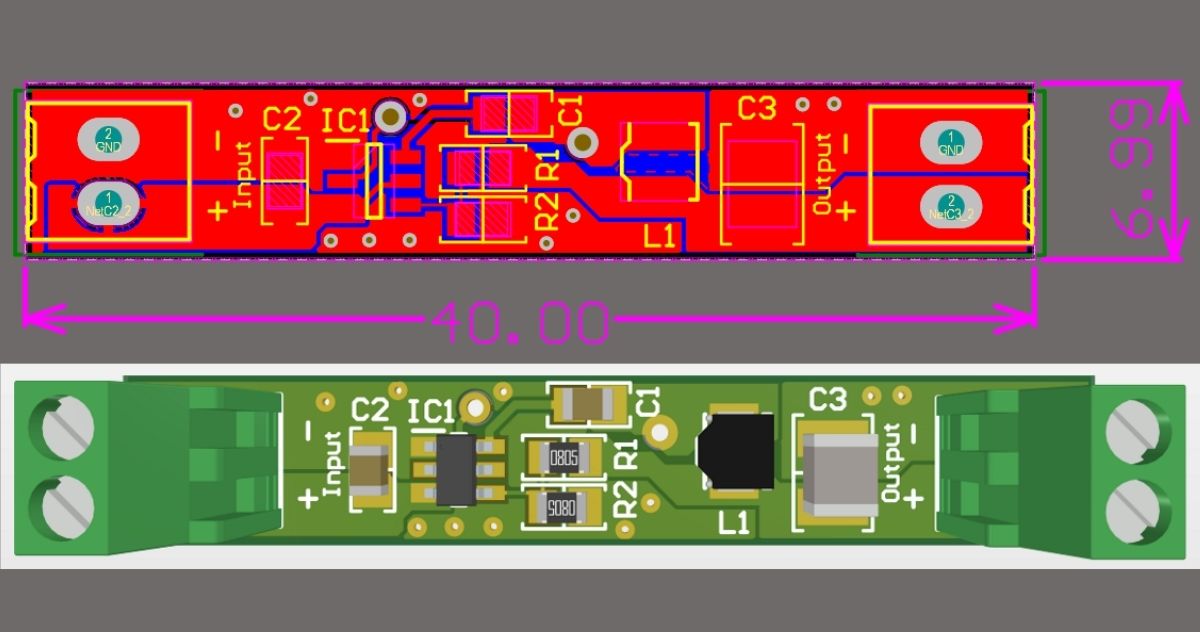
After my Reddit AMA with Altium, there were a lot of questions from students and graduates asking what they could do to improve their skills and show they are worth hiring. I suggested working on projects that would help cement their skills as well as show their experience with design - I wrote an article with suggestions on getting started on projects and some project ideas. In this article, we’re going to look at the implementation of one of the power supplies in that project.
I figured that since I’ve designed hundreds of switched-mode power supplies, me just running through design is probably not going to be perhaps as educational or informative as it could be on the pitfalls or issues associated with designing a power supply. They seem trivial on the surface - add a few caps, IC, inductor and a few resistors right? The current loops on a switched-mode power supply and component selection, however, is non-trivial. I thought it would be more interesting to hire a freshly graduated electronics engineer without much experience in power supply design and have him design a power supply with just the requirements listed in the student project ideas article.
You can find the final PCB design for this project on my GitHub page; it’s released under the open source MIT license. As this design has been completed by someone else, the schematic style is a little different from my usual projects. You’ll also find all the components used in this design in my extensive open source Celestial Altium Designer Library.
Power Supply Requirements
The task is to design a standalone DC-DC buck converter. To understand and be able to design a voltage supply is a crucial skill for anyone interested in electronics, from a hobbyist/maker level to full time professional. Switching power supplies are very common as they offer high efficiency, and therefore do not typically require thermal management as a linear supply would. Implementing a switched mode power supply is as mentioned before more complicated than a linear supply - with a linear supply you can’t really go wrong.
Power supply requirements:
- Input Voltage 7.0 ~ 14.0V
- Output voltage 5.0V
- Output Current 1.0A
This is a typical requirement for a wall power adapter to 5V supply. You probably have a power adapter for some device you no longer need around your house somewhere that you can use to test this if you don’t have a lab power supply. You could also use a 9V battery for supplying power. The input range of 7 to 14v offers a wide range of compatibility with various wall supplies as well as different battery chemistries.
5V is a very common input power requirement, especially if supplying power over a USB cable. The output current of 1A is sufficient for most light load standalone projects you can build.
I left the graduate engineer to decide how he would implement the power supply with the only limitation that the components should be readily available from major supplies like DigiKey and Mouser. There’s not much point building a power supply with components that cannot be easily sourced!
He chose to base his power supply design around a Texas Instruments TPS561208DDCR. This buck converter IC easily meets the requirements as it has 4.5V to 17V Input voltage and adjustable output voltage from 0.76 V to 7V and 1A maximum output current. Also, this IC fulfils the other requirement of being readily available, as it can be purchased from all the major distributors.
At this point, I’ll note that when designing a 1A supply I would typically choose to design a power supply around an IC with a higher current rating, so my circuit’s maximum power rating is still well within the margins of the regulator IC. This should not be an issue in reality, as there is some capability to push a supply beyond its ratings - but I try not to run any IC right on the ragged edge of its ratings at any point in time.
Beyond the requirement for a component to be well-stocked, you should also try to avoid the use of components with the labels of “Not recommended for new designs”, “NRND”, “No longer available” or “obsolete”. These labels mean that these components are either approaching or already at the end of their production life and probably will not be manufactured in the near future if manufacturing has not stopped already. While there may still be stock available at the moment, the life of your project is limited to the exhaustion of that supply before it needs to be redesigned, and possibly go through certification again as a result of the power supply change. This redesign and recertification can be very expensive and time-consuming, potentially leaving a product you have designed in a limbo state without any stock to sell, or the ability to manufacture more units.
If you want to check the availability of the components, you can check each distributor’s stock individually or use Octopart.com to check them all at once. Octopart® will allow you to see how well a component is stocked globally so that you can get a feel for stock levels and access to stock.
Schematic design
Before we dive into what the graduate worked on, I will mention that most Texas Instruments regulators are available in Web Bench. This online platform will calculate a schematic for you to meet your requirements. While it might be incredibly tempting just to implement it directly, it’s worth noting that the simulations and models used on web bench have been known to have issues in the past. You should read the datasheet if you use any calculation tool for any aspect of your circuit design and make your calculations based on the specifications and formulas contained within. Not only does this allow you to double-check the calculated design, but it also allows you to double-check the datasheet and also get a more in-depth understanding of what the regulator is doing. Understanding why a component of a certain value or current rating was used is critical to understanding how the regulator functions, and therefore what layout considerations there might be.
As a first step into the schematic design for the TPS561208, the output voltage resistors were chosen to set the output voltage to 5V. The resistors can be calculated with the formula:

If calculating differential equations isn’t your strong suit, you might like the Symbolab calculator which provides step by step solving of the equation or use Wolfram Alpha.
Choosing the appropriate resistor values can be challenging, as choosing low values would mean that the converter is less susceptible to noise. Still, at the same time, the efficiency with light loads would decrease. The value for the R2 resistor was selected as 10k Ohm from the recommended table in the datasheet, and then the R1 value was calculated from the formula:


As a 55.104k Ohm resistor is not a standard value, 56.2 kOhm value was chosen, which provides us with an output of 5.08 V.
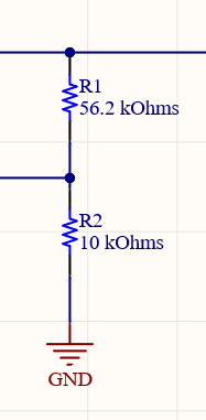
Output voltage resistors
The datasheet recommends an input capacitor of 10 uF or larger, so a capacitance of 22 uF was chosen as many 9V wall adapters are quite noisy.
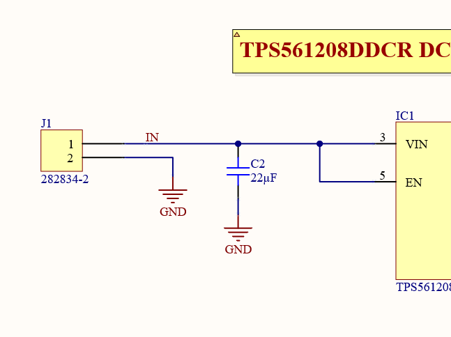
Input capacitor
The inductor selection can become quite complicated, so the value was chosen from the recommended component values table:
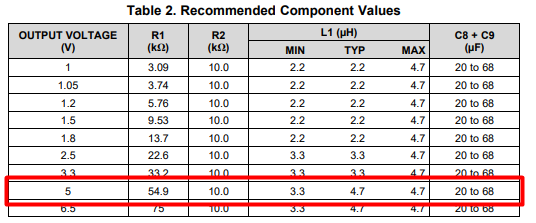
Recommended component value tables
Although, do not forget to choose the inductor which is rated for more than 1A of saturation current and rated current so that you will have a stable inductance value and to ensure your inductor will not get too hot. Typically a datasheet will also contain a formula to calculate the current through the inductor, as the load on the circuit is not necessarily the load on the inductor and this can be a critical factor when selecting the right component.
The graduate also chose the recommended output capacitor values from the tables in the datasheet too. The output capacitance is recommended from 20 to 68 uF for a stable converter. In this design, a single the middle value 47 uF capacitor was chosen. I like that he is playing it safe and following the datasheet’s recommendations. Most of the major suppliers such as Texas Instruments and Analog Devices, have extensively tested their devices and provide excellent recommendations in their datasheets. When it comes to power supply design, you should have a good understanding of the function, and a good reason to deviate from recommendations in the datasheet. You might choose to add significantly higher capacitance if you have a rapidly changing load on the supply, for example.
In addition to the input and output capacitors, a bootstrap capacitor is required for a proper operation. The manufacturer recommends the value of 0.1 uF ceramic capacitor.
The last thing to choose is the connectors. There is a huge variety of connectors options available to suit every need on the market. The graduate decided to look through the Celestial library and to find the one he liked, as there was no requirement stated for connectivity, and settled on 2-pin terminal blocks from TE Connectivity to make connecting wires and testing the board easy. Terminal blocks are also easy to source, and also other terminal block connectors with a common pinch of 2.54 mm can easily be substituted. I would have been equally happy with a USB type A connector on the output; however, the terminal block does make testing a lot easier.

The designed schematic for TPS561208DDCR buck converter
PCB Design
I didn’t provide any input to my graduate engineer when it came to the PCB design, and he had progressed through the schematic design very well without falling into any traps, so I was interested to see how he went with the PCB design. PCB design is where you can go wrong with a switched-mode design very quickly. When I was first learning how to design power supplies, I certainly made mistakes which caused highly unstable power supplies that would fry themselves seemingly without any reason - that reason, however, was poor board layout. Switched-mode power supplies are unforgiving if they get into an unstable state, and will let the magic smoke escape pretty quickly as things begin to go horribly wrong.
His first board design looks excellent aesthetically, it’s compact and flows from left to right beautifully… but it’s probably going to perform poorly.
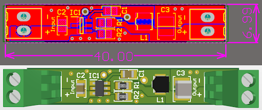
The PCB designed by the graduate engineer
Although the PCB looks okay, there were several problems with it:
- Not following the recommended layout and design tips from the datasheet. Texas Instruments typically provide extensive layout advice in their datasheets, and it should be heeded. You might think the recommendations for layout in the datasheet are targeted towards less experienced engineers, but you can ignore them at your peril. The advice is usually very sound, and going to set you on a path to a great layout, even if it’s not particularly convenient to fit onto your desired board shape/area.
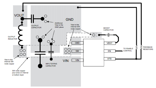
The layout example of the PCB from the datasheet
- The switching path of the inductor and current loops were not routed properly, which may lead to excessive crosstalk and EMI problems. The current loop layout of switching voltage regulators can drastically impact your performance beyond regulator stability, and cause the regulator to be the noisiest thing on your PCB. This can be a fantastic way to fail your EMC certifications with style, and send you back to create a new board revision that fixes the issues.
The two current loops, input (Blue), and output (Red) in the first pass design look like this:

Input and output current loops of the first DC-DC buck converter design
For EMC purposes, the current path through the regulator should be kept as short as possible. In this design, the output current path is too long. This will lead to additional noise, switching crosstalk and EMI problems. The current loops should be as short and wide as possible to minimise the radiated emissions.
To correct the PCB layout, my primary advice was to review the datasheet and study how current flows in the recommended layout. The current flows in a circular pattern, without crossing back over itself, providing loops of current - rather than a scenic detour that crosses over itself. Part of this is ensuring the shortest paths from the IC to critical components such as the input and output capacitors and the inductor as mentioned before. The grounds from the capacitors should terminate as close to the ground of the regulator IC as possible, as should the positive voltage pins.
I also suggested routing every trace without relying on polygons and then pouring the polygon over the top of those traces. By routing the trace manually first, you can visualise and get a good feel for where the current path is. This is most critical on the ground net as I find many less experienced engineers will add a ground pour and assume everything is good, without looking at how their ground is connected or flowing.
The first step of the layout correction was the right component placement. The component placement was taken from the recommended datasheet layout with slight modifications to accommodate the components chosen.
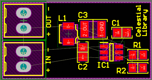
Component placement by following the datasheet recommended layout and design tips
The second step was to manually route all the traces, without placing polygons (even ground). This step is needed to follow the current flow through the input and output loops and through the circuit. In this way you can see how long the loop will be and in what direction current will flow:
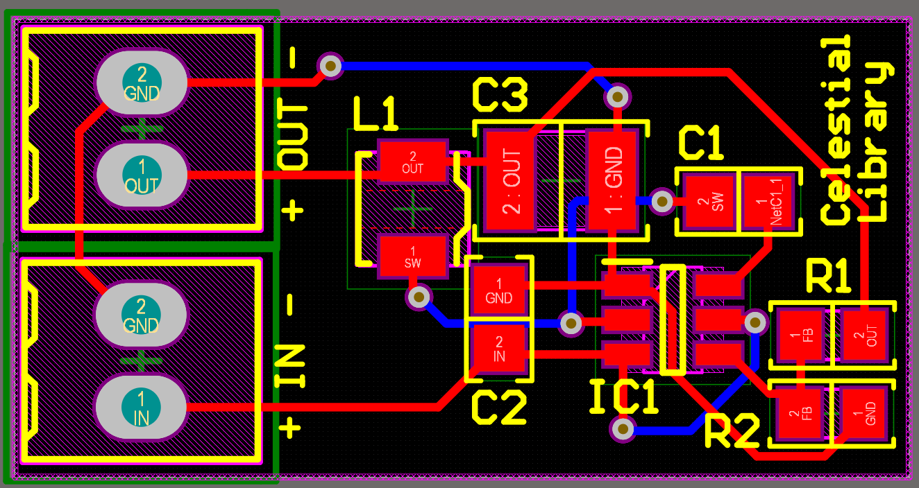
Manually routed PCB
After routing manually, you can check the current loops:
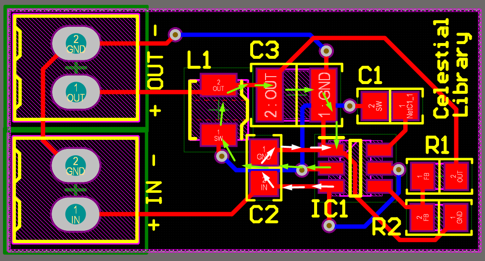
Although the input loop is not changed that much, the change in output loops is much improved
This resulted in a far more functional-looking layout. The third step is to add polygons to the input and output loops so that we would achieve as low impedance as possible:
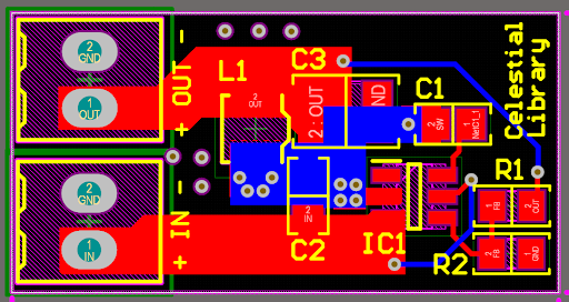
Polygons added to the input and output current loops
Finally, the top and bottom layer ground planes were added to the design. The nets are already routed manually, so we know that his design will have a good ground current path - the polygon is merely adding more capacity and shielding.
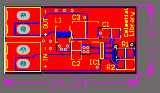
The PCB design of proper step down voltage regulator layout
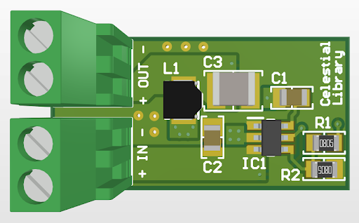
3D view of the PCB proper step down voltage regulator layout
After the corrections for the PCB layout, the output current loop becomes much smaller, and both input and output current loops are facing the same direction:
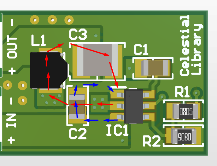
The current loops of the final layout
Conclusion
The design of a simple DC-DC buck converter is not as simple as dropping a linear regulator into a circuit. The wrong component selection or layout can bring additional noise to your PCB, excess electromagnetic radiation and at the worst, an unstable regulator that performs poorly or burns out instantly under certain load conditions.
When designing the schematic of adjustable output voltage regulators, you need to choose the output voltage divider wisely. Choosing high resistance values for the voltage divider will increase the efficiency of the regulator at light loads; however, the susceptibility to noise will increase. Choosing low resistance values the effect will be vice versa.
The input capacitor selection can be quite complex, taking into account input supply voltage ripple and noise, as well as the current demands, particularly how fast those demands shift, of the regulator. The input capacitor will also influence the conducted noise levels on the supply voltage, which if conducted into cables, could cause EMC certification challenges.
The inductor selection on a switched mode voltage regulator is highly critical, ensuring that it will not be saturated and has the correct inductance to ensure efficient operation. Phase margin and other technical aspects can also come into play and affect the stability of the regulator, however that could be a topic for an in-depth article by itself.
The output capacitor type and parameters will have a significant impact on the conducted noise on the output voltage rail. Using the wrong capacitor type might provide you with plenty of capacitance but still provide a very high voltage ripple on the output without much smoothing.
The PCB layout is also critical for the buck converter. Keep traces as short and as wide as possible for current loops. Ensure both pins for input and output capacitors have an easy path back to the regulator. Current loops should be short, circular, and flowing in the same direction to reduce EMI.
Would you like to find out more about how Altium can help you with your next PCB design? Talk to an expert at Altium.