Should You Use Power MOSFETs in Parallel?
The intrepid power systems designer should know all about MOSFETs and their particular electrical peculiarities, but working with arrays of MOSFETs can be another beast. One arrangement you might see in a power conversion system is to place multiple power MOSFETs in parallel. This shares the load among multiple MOSFETs with the goal of reducing the burden on the individual transistors in your system.
Unfortunately, MOSFETs (and nonlinear components in general) do not simply divide up the current among themselves in the same way as, say, a group of resistors in parallel. Just like in a single MOSFET, the heat now becomes a consideration as it determines thresholding behavior in MOSFETs (again, this applies to any real nonlinear circuit). To see how these components interact with each other in this arrangement, we need to look at the parasitics that exist within a MOSFET chip and between power MOSFETs in parallel so that you can prevent components from destroying themselves.
Working with Parallel MOSFETs
Like any other component, be it linear or nonlinear, multiples of the same component or circuit network can be connected in parallel. This is also true for power MOSFETs, BJTs, or other groups of components in your schematics. For 3-terminal devices like MOSFETs, where power must be supplied at two terminals, the configuration involved may not be so intuitive. The schematic below shows an example from a power converter where four MOSFETs are hooked up in parallel on the converter’s output side.
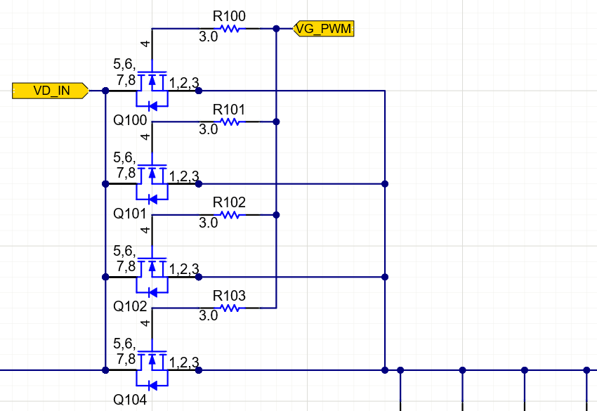
Note that there is a small resistor connected to the gate on each MOSFET (I’ll explain why in a moment). There is also a single gate pulse from a synchronous driver at the VG_PWM port, which is used to switch each MOSFET simultaneously. In other words, these MOSFETs are not driven in a cascaded manner; they are driven such that they all switch on and allow current to flow at the same instant.
The advantages of hooking up MOSFETs in this way is that they can each be used to provide lower current to a load. In other words, the total current is split evenly among each MOSFET, assuming they have the same ON-state resistance. This allows each power MOSFET to provide high current while still having high current margin, which then reduces the amount of heat they generate.
Two points aren’t included in the typical analysis of power MOSFETs in parallel: parasitics in the MOSFET. Parasitics already create bandwidth limiting, filtering, or resonance effects in real components. However, when we have multiple power MOSFETs in parallel being driven with a high-frequency PWM signal, their parasitics can interact with each other and increase the possibility of an unwanted oscillation during switching. This would then appear as a glitch on the system output and can lead to excessive heating in the victim MOSFET.
Simulating Power MOSFETs in Parallel
When you have multiple power MOSFETs in parallel, and you want to simulate how parasitic oscillations might arise, you can build a simple circuit with a gate driver for your particular MOSFETs. Make sure you’ve attached the appropriate simulation model to your component, where the model includes stray capacitance between the various pins in the component. An example circuit with a load on the source side is shown below.
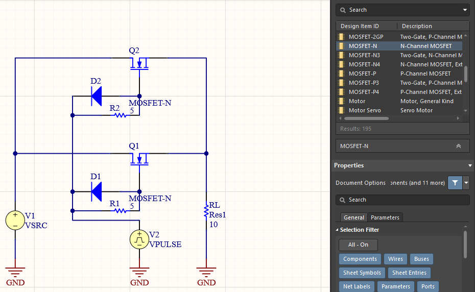
I’ve used a VPULSE source from the Simulation Sources.IntLib library to model a PWM driver. The diode D1 is a 1N914 diode arranged in a gate driver circuit for an NMOS transistor. From here, you simply need to perform transient analysis to examine the current and power delivered to the load by the MOSFETs.
Note that there are a few quantities that are of interest in this simulation:
- PWM rise time: this determines the bandwidth of the PWM signal and should be matched to the specs for your MOSFET
- PWM frequency: a PWM signal with higher frequency will see lower impedance from the parasitic capacitance, which injects more power into the parasitic feedback loop, possibly driving the system into resonance.
- Gate voltage: Because a MOSFET’s response depends on the magnitude of the gate voltage, so will any parasitic oscillation that arises when the PWM signal switches the parallel array.
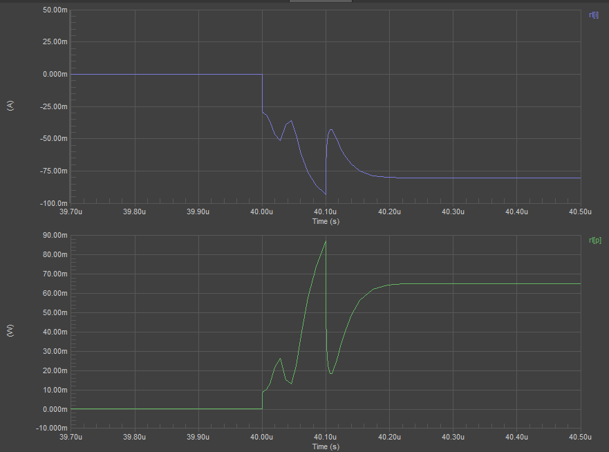
You can easily spot the effects of parasitic inductance and parasitic capacitance in a transient simulation. The example below shows results for the pair of MOSFETs above when the parasitic capacitance and inductance are included in the simulation model. Note the large glitches that are clearly seen in the time-domain response as the PWM signal switches.
Damping Unwanted Oscillations and Temperature Rise
As was mentioned earlier, these unwanted oscillations can arise in different MOSFETs in the array if there is a temperature imbalance. In other words, the condition for resonance in one MOSFET can be different than in another MOSFET. If one MOSFET experiences strong oscillations before the other MOSFETs for a given gate voltage, then the component can destroy itself. Therefore, it’s best to keep these components at the same temperature if they are connected in series. This can be done with a large heatsink or a plane layer below the components in your PCB layout.
The other way to modify the conditions for resonance is to place a gate resistor in the driving circuit (see above, where a small 5 Ohm resistor is included). MOSFETs in half-bridge LLC resonant converters may have a very large resistor connecting the sources and gate to provide high damping between these two ports. You can experiment with these resistor values to examine how they affect damping in the parallel circuit.
Analog simulation is a central part of circuit design, including for power MOSFETs in parallel. The circuit design and PCB layout tools in Altium Designer® give you a complete set of features to help you create your circuits, simulate signal behavior, and create your PCB layout. Once you’ve qualified your schematic design, you can share your design data on the Altium 365® platform, giving you an easy way to work with your design team and manage your design data.
We have only scratched the surface of what is possible to do with Altium Designer on Altium 365. You can check the product page for a more in-depth feature description or one of the On-Demand Webinars.
