Buck Converter Simulation in Altium Designer
Any new PCB you want to build will need a power source, and the power you need to provide is often stepped down from a noisier unregulated source. An example is an output from a full-wave rectifier, which will contain some residual ripple at the output port. Another possibility is the noise from an upstream converter. In other cases, you are drawing power from a battery, and the battery’s voltage/current output will change over time or with temperature.
No matter the situation, you can usually find a suitable DC-DC converter or LDO from a distributor, and you can easily add it to your board. When designing high power circuits (usually very high voltage and/or current), you’ll need to create a regulator from scratch and place it in your PCB layout. As part of buck converter design, you can easily run a buck converter simulation directly in Altium Designer’s schematic editor. Here’s how you can access these features in the newest version of Altium Designer.
Starting a Buck Converter Simulation
The schematic editor in Altium Designer includes a SPICE-based engine for creating simulations directly from your design data. Other platforms provide similar tools, but they will eventually require you to export your design data and simulation data to an external program for analysis. Instead, you can do everything in Altium Designer, including immediately capturing your schematic as a new PCB layout.
After you’ve completed your buck converter circuit, you can access the schematic editor’s simulation tools in the new Simulation Dashboard feature in Altium Designer. You’ll need to complete the following steps to run a buck converter simulation for your circuit:
- Define your voltage sources. Simply use the Simulation Sources.IntLib component library in the Components panel to access a range of simulation sources. You need to simulate a DC input (or rectified AC input) and a PWM source for switching the high-side transistor (see below for more information).
- Place probes for desired measurements. The SPICE engine in Altium Designer will return current, power, and voltages for different nets and individual components. You can also place voltage, current, or power probes in your schematic to gather measurements on specific nodes or components.
- Create a simulation profile. With the schematic editor open, click on the “Simulate” button on the main menu bar. You can now access all the SPICE simulation features by clicking Edit MixedSim Profile. You can rename your profile as you like and configure a number of other settings.
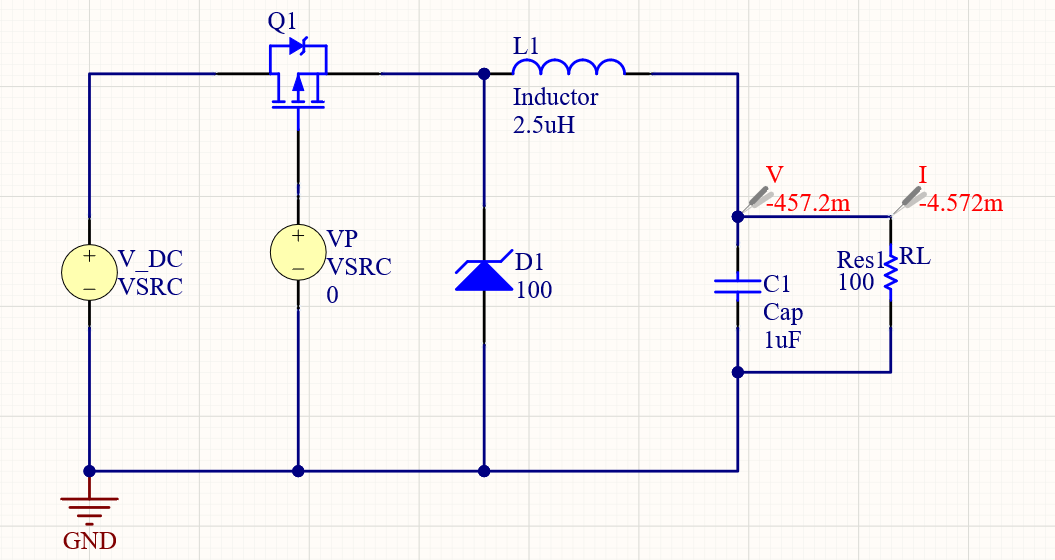
The goal in a buck converter simulation is to examine how the duty cycle of the PWM signal, the load, and any other components affect the power output from your buck converter. You should also examine ripple, ideally with an AC source and a rectifier bridge. It’s a good idea to start with the basic buck topology (see above) and add more features once you’ve chosen the right components.
Modeling the PWM Source
The PWM source can be modeled using a pulsed source. I’ve placed a voltage source in the above circuit diagram, but you need to source a specific current (voltage) into the base (gate) in the BJT (FET). Here, we're using a generic PMOS transistor model, so we will source a voltage from our PWM driver. In a simulation, you can place a current source as VP, or you can place a resistor in series with VP. Either method can be used to define a PWM source to switch the transistor in this circuit.
Note that all AC or switching sources have some maximum current that can be drawn by a downstream device, so it doesn’t hurt to use a current-controlled voltage source to examine your power converter circuit’s behavior when driven with a more realistic PWM driver.
The switching frequency and duty cycle of the PWM source can be modified by opening up the voltage source’s simulation information from the Properties panel. Simply adjust the pulse width (duty cycle) and period (frequency) to tune your modeled PWM source (see the settings below).
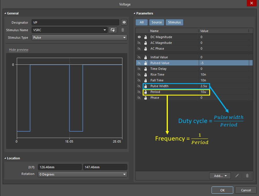
I’ve used a somewhat fast rising pulse edge of 10 ns in the above simulation settings. This is sufficient for modeling purposes as the pulse width and period are much larger, and we don't really need to include the rise/fall times in the calculation of frequency and duty cycle. If the rise/fall time were much slower, then we would need to include them as they become comparable to the pulse width and period. Once the PWM source is defined, you can enable some analyses to perform in your simulation profile.
The Simulation Dashboard
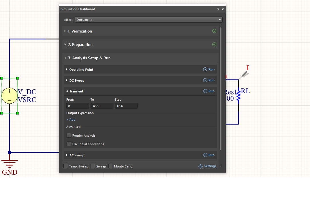
Altium Designer's new Simulation Dashboard is a central location where designers can cue up mixed-signal simulations for their circuits. The Dashboard is accessible under the Simulate menu within the Schematic Editor. From here, you can run the four primary types of simulations you'll need for most circuits:
- Operating point simulations
- DC sweeps
- Transient analysis
- AC sweeps (a.k.a., frequency sweeps)
The Simulation Dashboard saves time as it will automatically check your design for simulation models and verify electrical rule checks. The image below shows my setup for a transient analysis simulation. Custom output expressions can be added to display electrical measurements in your simulation results window.
Results
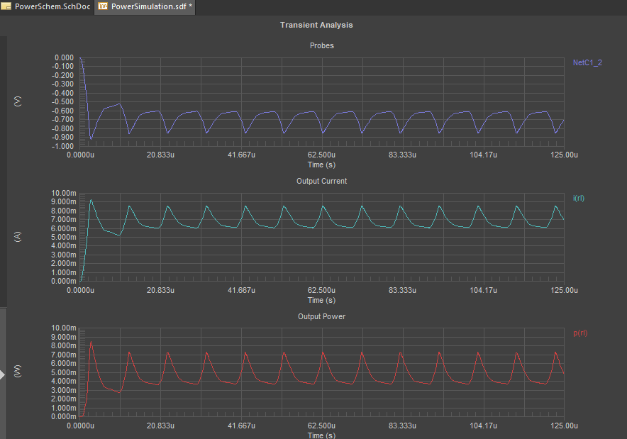
The image below shows my current and power results on the output from my regulator. As we can see, this regulator provides ~mW of power at ~25% duty cycle (100 kHz) at 7 mA of current (V1 = 4.8 V, stepped down to ~700 mV). The converter is operating in the discontinuous mode as the inductor current drops to zero during commutation (not shown in the graph below). The switching noise on the output is still rather high, although we are running above the resonant frequency of the LC network in this circuit. The top graph (output voltage) shows an apparently very large swing, giving a similar magnitude swing on the output current.
What to Examine in a Buck Converter Simulation
The important point to examine in a buck converter simulation is the transient behavior. You don’t need to go so far as pole-zero analysis as you can prove, simply due to the circuit's negative feedback, that the output from the buck converter will enter a limit cycle. Therefore, you only need to examine how the oscillating PWM signal transforms the output voltage. This is best done in the time domain using simple transient analysis.
Note that, unless you have placed EMI filters on the input/output and using a PFC circuit, there is no reason to extract the transfer function as long as the inductor is sized correctly. For the desired ripple current, the required inductor size, PWM parameters, and input voltages should obey the equation below. Note that this is normally defined in terms of the voltage drop across a MOSFET:
Again, you should generally be working with sufficiently low frequencies that you won’t need to worry about bandwidth-limiting effects in your BJT/FET. To learn more about selecting the right PWM frequency and edge rate, take a look at this article.
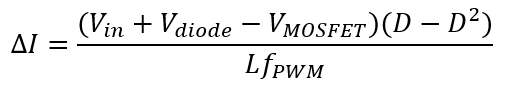
The above equation assumes continuous conduction mode, which I'll discuss more in an upcoming article. In my results, the peak-to-peak ripple in the output current was ~1.6 mA. This is very large, amounting to ~24% of the average current. From the above expression, we need to increase the size of the inductor and increase the frequency to stabilize the output current. The graph below shows some results, where the output current has been stabilized using a much larger inductor of 100 uH and 1 MHz switching frequency with the same duty cycle of 25%. Here, we get a slower transient response to a stable output, but we have very low noise of about 0.006 uA, or about 0.4% of the average output current.
Here it's important to note that, because we're in the discontinuous mode, the output will voltage is now also a function of the inductance. This is not the case in the continuous mode. Therefore, we should focus on how to avoid the discontinuous mode when redesigning this regulator. I'll cover this in a later article as it enables much easier converter design, particularly when high power is needed at the load.
Moving on to Your Layout with Schematic Capture
If you’re happy with your power converter circuit and you’re ready to interface it with the rest of your system, you can take a few paths:
- Integrate your circuit into hierarchical schematics. If you have a higher level schematic, you can bring the converter into a larger system using the hierarchical design features in Altium Designer. Click here to see how this works for complex systems.
- Create a PCB layout. If the converter will operate on its own, all you need to do is use the integrated schematic capture tool to create your layout. Click here for a guide on creating a new layout from your schematic.
When you’re ready to layout your new board, you’ll simply create a PCB and use the integrated schematic capture tool to import your components into a new layout. You can now start arranging your components in your new layout.
If you’re familiar with switching converters, you know they can create significant noise in your circuits. The basic mechanism is due to a strong magnetic field during switching in the FET, which then induces a current somewhere else in the circuit. The second mechanism is a ripple problem, which can propagate through the converter and appear as noise on the output. EMI induced anywhere in your buck converter circuit, whether through switching noise or an external EMI source, can appear on the output signal if the output stage is not filtered. You can read more about suppressing noise from switching converters in this article.
Share Your Simulation Models and Schematics in the Cloud
If you're collaborating with other designers on a buck converter simulation, you can use the complete set of sharing tools in Altium 365 to store and access simulation models for your components and simulation models. You can share your schematic sheets as individual files or in a project so that others can access your simulations. You can also share individual .subckt models for specific components in a cloud environment. You can also access your .subckt models when creating a new component. All of this can be instantly imported into Altium Designer without manually downloading and organizing your simulation files.
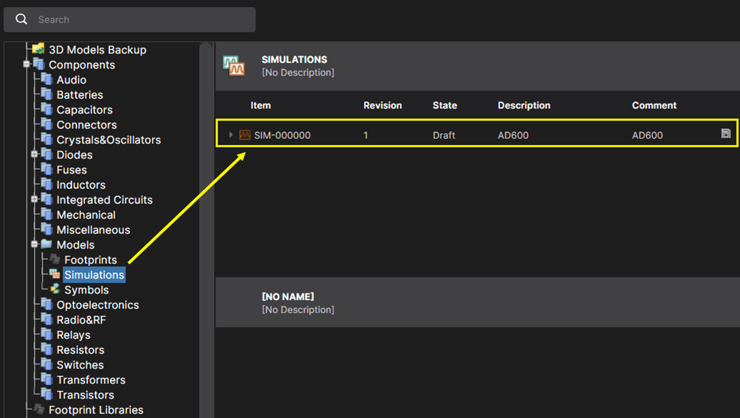
The above image shows the web interface for Altium 365, where users can organize and store their simulation files for components in a secure cloud platform. SPICE simulation models can be stored along with footprints and symbols, and sourcing data can be attached to real components to help speed up procurement. Read this recent article to learn more about sharing your SPICE simulation models in Altium 365.
When you need access to the world’s best circuit design, simulation, and PCB layout tools, try using the full suite of design features in Altium Designer®. You’ll have everything you need to create a new board for your DC-DC converter, run a buck converter simulation, and find your board's components. The Manufacturer Part Search feature allows you to source the component models you need for your design direct from major distributors and component manufacturers.
Altium Designer on Altium 365 delivers an unprecedented amount of integration to the electronics industry until now relegated to the world of software development, allowing designers to work from home and reach unprecedented levels of efficiency.
We have only scratched the surface of what is possible to do with Altium Designer on Altium 365. You can check the product page for a more in-depth feature description or one of the On-Demand Webinars.
