PCB Routing Guidelines for DDR4 Memory Devices
In 2014, the fourth-generation of DDR RAM (DDR4) was introduced, offering reduced power consumption, increased data transfer speeds, and higher chip densities. DDR4 RAM also featured improved data integrity with the addition of cyclic redundancy checks on write data and on-chip parity detection. With notable improvements in speed, performance, and bandwidth, DDR4 memory deserves special attention.
DDR RAM devices can be a difficult to work with due to the large number of signals that must be routed on a PCB or SODIMM card, but these memory devices are not going away anytime soon. In fact, now that DDR5 and DDR6 are on the horizon, having a solid foundation in DDR4 routing guidelines will give you a head start if you ever plan to use these more powerful memories in your system. If you're just getting started learning about DDR routing or you need to get a quick refresher, we've compiled the essential DDR4 routing guidelines in this article for your reference.
DDR4 Routing and Design Rules
Before you route a single trace on your DDR4 bus, it's critical to know the functions of each signal and their impedance values. If you start searching for impedance values and signal functions in DDR4 modules, it can be difficult to find consistent answers. This is because many modules and controllers will use on-die termination so that the termination impedance at the various pins can be adjusted. However, you will still want to match the driver impedance to the trace impedance and terminate appropriately.
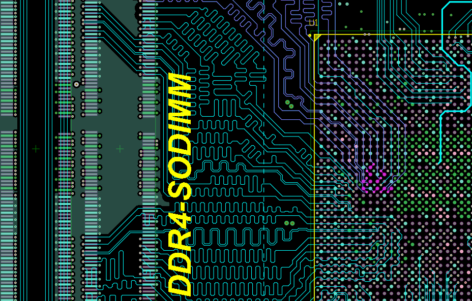
The image below shows the various signals involved in DDR4 routing between a controller (CPU, FPGA, etc.) and DRAM modules. Note that these guidelines apply whether you route through an edge connector to a SODIMM card or directly to modules mounted on a PCB. SODIMM cards are the standard method for routing to DRAM modules in computers, while a single-board computer or SoM will have the DRAM modules directly on the PCB. Only the DQS and CLK (clock) signals are differential pairs, the other signals are single-ended traces.
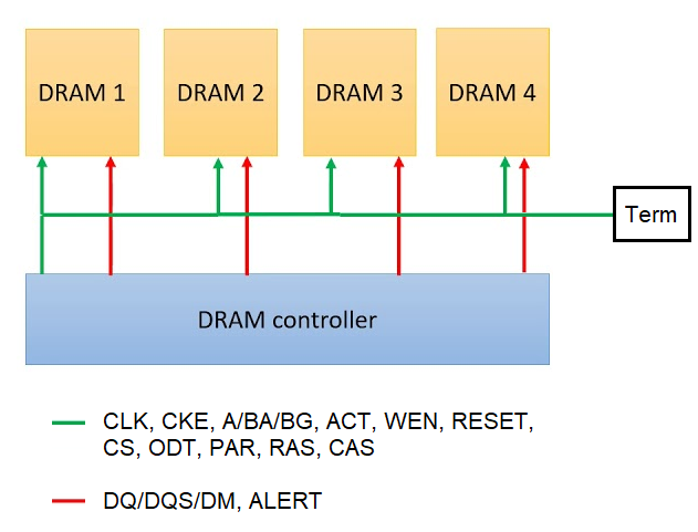
This routing topology is called fly-by topology, which was originally introduced for use with faster DDR3 modules. Here, we need to consider termination for the traces used in the above image, as well as the target impedance and skew limits between various traces.
DDR4 Impedance Values
Although you'll typically see a 34 Ohm or 40 Ohm single-ended trace impedance value in many designs, some modules will support as high as 50 or 60 Ohms single-ended impedance. Note that there is no single impedance because the driver's output impedance value will depend on the drive strength and the receiver input signal level. The differential pair impedance values in the above topology are typically doubled the value of the single-ended impedance. This will be specified in your controller's datasheet in the DDR4 interface specifications. Note that the driver output impedance may be configurable among various values. 34, 40, and 48 Ohms single-ended impedance are common, and each of these will have a specific corresponding differential pair impedance.
DRAM module vendors and controller manufacturers provide plenty of guidance on determining the optimal impedance values based on the required drive strength. Be sure to check your datasheets for all components for guidance, but you should also run layout-level simulations to verify signal integrity. You can use a field solver with a built-in impedance scanner to calculate any impedance violations once you complete your layout.
Termination
In the above image, you'll notice a termination circuit (labeled "Term") at the end of the last module. This refers to a specific circuit used to terminate the single-ended and differential pairs used in routing each of the above signals. Single-ended pairs will use series termination to the VTT power bus after the final DRAM module. The CLK differential pair termination circuit could vary for different modules, so be sure to check the datasheet for your modules to ensure correct termination. One possibility is to use a parallel load termination. Another possibility for some DRAMs uses a pair of resistors and a capacitor to VDDS, as shown below.
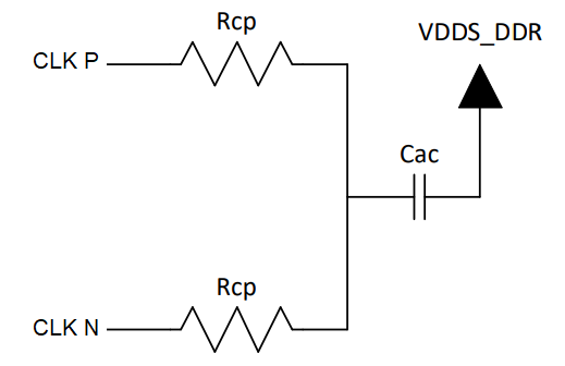
In the above circuit, Rcp and Cac will be specified depending on your driver strength and on-die termination resistance. A typical value for Cac is 0.1 uF, and Rcp will be the single-ended impedance specified for the trace. Note that some modules will have selectable on-die termination. This is configured when the module is first brought up to power via the ODT pin on each module. Note that the ODT trace extends from the controller to all modules, so each module should have the same termination impedance on applicable pins.
Allowed Skew
Because fly-by topology is a parallel bus with source-synchronous clock, you'll need to apply length matching between signals in the data bus. Not also that this applies between two traces in a differential pair. The following routing guidelines apply:
- Differential pair skew: The skew between each trace in the pair should be as small as possible to ensure sufficient elimination of common-mode noise at the receiver for the DQS and CLK signals. The data sheet for your receiver module will give recommended maximum skew values for differential pairs.
- Skew between signals: The skew between different signals in the bus should also be timing-matched, but the allowance for skew is much more generous. Some datasheets will specify something like 1 mm length tolerances, which equates to several ps of timing margin between signals. It's best to play it safe and just timing match as close as possible across the bus.
Clamshell Topology
DDR4 DRAMs can operate with either clamshell topology or fly-by topology. Both topologies involve advantages and disadvantages. The clamshell topology uses less board space and two layers but requires a complex routing plan. Crowding the routing between the top and bottom layers under RAM devices can lead to routing congestion and longer stub traces. In contrast, the fly-by topology allows for easy routing and provides the best signal integrity. However, fly-by topology—with one layer of in-line RAM devices—requires more space. Ultimately, deciding which of these options is best for your layout is dependent on the need for your device.
Planning Your DDR4 Routing
DDR4 routing channels can get very congested due to the large number of address and data signals being routed between the processor and DRAM modules. Because SODIMM DRAMs typically only have 4 layers, these buses can get very wide. Typically, the DDR4 routing guidelines found in a component datasheet will focus on placing everything on one layer, or placing each bytelane on its own layer. This is a good plan from a stackup and routing perspective as you need to maintain controlled impedance in the design. Placing everything on one layer allows you to define a specific trace width to ensure fixed impedance. In addition, this helps with length matching across the bus as all your signals will have a definite propagation delay on that specific layer.
Example With Modules
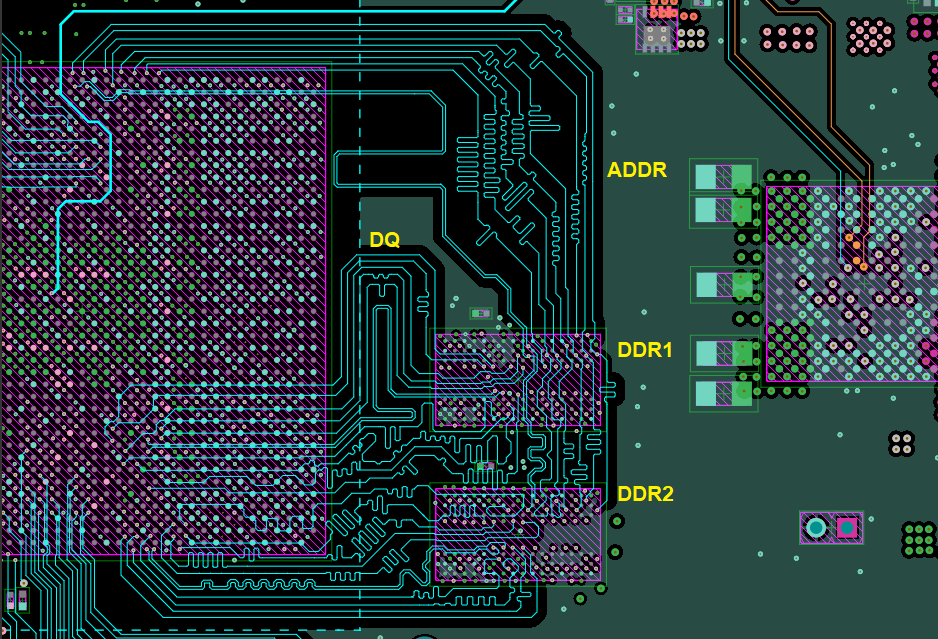
The example below shows a good example with the CLK, DQ, and ADDR lines for a byteline. Here, the lines are all being routed on the same layer as striplines with delay matching applied. The ADDR lines are being routed together along a lane along the top-right of the image, and the DQ lines are sent between the processor and module horizontally. It's a good strategy to plan out the space required on multiple layers, and make sure to route the DQ, DQS, and DM signals within a given byteline group on the same layer to avoid layer-to-layer propagation delay differences.
SODIMM Card
If you're routing to more than one SODIMM card, you can use the example shown below. Here, the SODIMM card slots are placed in parallel so that traces from the processor can extend across pads from each card slot. This can also extend across two layers, as shown with the different colored traces below. Note that the layers below are both internal with stripline routing.
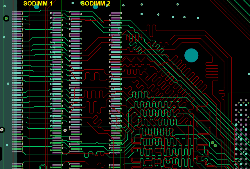
Note that, in the above image, vias are used to make the transition between layers after a route hits a SODIMM connector pad. These vias are only transitioning between two nearby layers, rather than across the board, so there will be some stubs above and below the transition region. Consider removing these stubs with back drilling to prevent excitation of a resonance in these leftover stubs. The other option is to place these routes lower in the board so that there is a longer via transition between layers, thus the leftover stub will be shorter and it will require higher frequencies to excite the lowest quarter wavelength resonance.
Trace Spacing and Length
Finally, spacing between routes and traces in differential pairs is for preventing crosstalk. Simulations can help here, particularly with the right field solver application, but you should still test the board with a prototype regardless of simulations. To plan for the amount of spacing between traces in layout, you would use the vertical distance to the closest return path (H) for a particular trace as a spacing factor. A very conservative practice is to set a minimum spacing of 5H between a CLK differential pair and other traces. For the Address/Command/Control and DQ/DQS/DM traces, this can be relaxed to a spacing of 3H.
Finally, pay attention to your propagation delay and attenuation along routing channels to determine maximum trace length. This should be based on maximum permissible loss, rather than on specific values in a datasheet as different PCB substrate materials will have different loss tangents. Always avoid routing two signal layers next to each other and route signal lines over their solid reference plane. As you build your routing plan, avoid routing signal lines over voids or reference plane splits to prevent radiated EMI.
Looking to the Future with DDR5
As of 2021, some companies are now hinting at upcoming releases of DDR5 modules. These modules are set to provide higher data rates with faster signals and tighter routing constraints. Many of the same ideas in DDR4 will remain valid, and you can implement these routing guidelines with the CAD tools in Altium Designer®. As these new modules are released onto the market, Altium Designer's complete PCB layout and routing toolset will be there to help you implement these guidelines in your board. When you install Altium Designer, you'll also have access to an example project with DDR4 modules on-board and SODIMM connectors to help you get started with DDR4 layout and routing.
When you’ve finished your design, and you want to release files to your manufacturer, the Altium 365™ platform makes it easy to collaborate and share your projects. We have only scratched the surface of what is possible to do with Altium Designer on Altium 365. You can check the product page for a more in-depth feature description or one of the On-Demand Webinars.
