PCB Trace Inductance and Width: How Wide is Too Wide?

Not all design rules are applicable in every situation, and they are often communicated without context. One particular rule for sizing traces is to always opt for wider traces when possible. Unlike many rules of thumb I’ve seen thrown about, this particular trace rule has some merit. However, when you need to control trace impedance and simultaneously reduce ringing, you need to carefully control the trace width to ensure transmission lines have desired impedance within some particular tolerance. Let’s take a look at the basic formulas for sizing traces and how to keep impedance within your tolerance range.
Impedance vs. Trace Width Formulas
I’ve brought up this point in previous articles specifically for surface microstrips and symmetric stripline traces. or microstrip traces, the IPC 2142 formulas are only highly accurate within a particular impedance range. You should use the more accurate Waddell's equations for determining the impedance of microstrip traces:
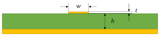
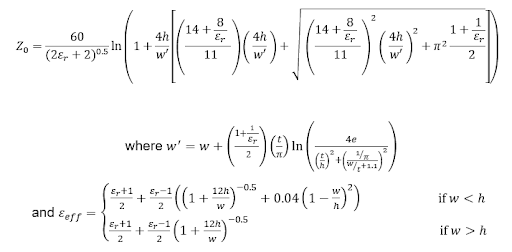
Similar equations have been developed for symmetric striplines, embedded microstrips, coplanar waveguides, and offset/asymmetric striplines. For now, I’ll confine the discussion to microstrips, but you can follow the process I’ll outline here for other trace geometries. Note that the above equation applies for single-ended surface microstrips that are isolated from all other signal traces.
What I’ll do now is use the above equations to determine the correct w value that provides minimum trace inductance per unit length for a specified trace impedance value. This need to minimize per-unit-length inductance is quite important, as the damping constant for any transient ringing signal (note that we’re not talking about reflections here) is inversely proportional to the PCB trace inductance.
Controlling PCB Trace Inductance and Impedance
If you look at the above equations, you’ll find that there are three important geometric parameters to consider when sizing traces and PCB trace inductance. In a real board, you’ll have some constraints on the value of h, which will depend on the board and layer thicknesses. You’ll also be limited in terms of trace thickness, which is proportional to the copper weight you use for your board. This means you can use the above equations in an optimization problem while taking the layer thickness and copper weight in your board as constraints.
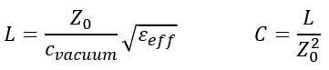
Here, the important parameter to determine is (w/h) for a given value of (t/h), substrate dielectric constant, and desired impedance value. There is an infinite number of pairs of these values that will solve the characteristic impedance equation. If you want to provide the greatest level of damping for transient ringing, then you need to determine the value of (w/h) that minimizes the inductance per unit length. This can be reframed as a problem of minimizing the effective dielectric constant for a given (t/h) value, substrate dielectric constant, and desired impedance value. The inductance per unit length, capacitance per unit length, substrate dielectric constant, and impedance are related as follows:
You could certainly attempt to do this graphically or through successive manual calculations. If you try to do this by calculating critical points from derivatives, you’ll end up with a set of products of transcendental equations (one piecewise and one continuous!) that must be solved numerically for various values of (t/h) and Dk. While this is a solvable problem in principle, it is clearly intractable due to the nonlinear piecewise nature of the effective dielectric constant and the fact that there are three relevant geometric parameters.
The best option to solve this type of problem is to use an iterative optimization algorithm to determine the values of (w/h) and (t/h) that minimize the PCB trace inductance per unit length. This type of problem can be easily solved with a gradient descent algorithm, an evolutionary algorithm, the Kuhn-Tucker method, or another nonlinear optimization algorithm. This allows you to define practical upper and lower limits on the value of (w/h). You can also set limits on the value of (t/h) and use this ratio as an optimization variable if you like.
Thankfully, this problem is simple enough to solve with the Solver tool in Excel. I’ve created a simple spreadsheet that solves the following minimization problem with Waddell’s equations and the inductance equation. In the following equation, a and b are constants that define practical maximum values of (w/h) and (t/h), respectively; these can be chosen by the designer:
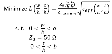
Here, the goal is to determine the values of (w/h) and (t/h) that minimize L (defined above) while holding the trace impedance constant. If you like, you can set a specific value of t from the copper weight, and the value of h can be chosen by the designer for a given t value (layer thickness).
Example 1: Varying Copper Weight and Layer Thickness
In this first example, I’m going to allow the copper weight and layer thickness (i.e., the value of the ratio (t/h)) to be an optimization variable. The substrate dielectric constant is Dk = 4. For the constraints listed above, I’ve chosen a = 5 and b = 2. For my results, I find that the minimum inductance is 290 nH per meter when (w/h) = 1.572332 and (t/h) = 1.213156.
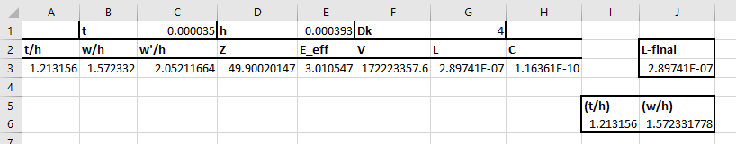
Optimization results for example 1.
In interpreting the results, it should be obvious that the trace width cannot be increased forever without changing the trace impedance; there is clearly some optimum trace width that optimizes the transmission line. The designer has one remaining parameter that needs to be chosen: the layer thickness h. Once this is chosen by the designer, the values of w and t can be easily determined from the calculated ratios listed above.
Example 2: 1 oz/sq. ft. Copper Weight, 4 Layer Board
This example shows a more practical situation. I’ve run the above optimization problem for a board with 1 oz/sq. ft. copper weight (trace thickness t = 0.035 mm) and a standard 4 layer board with equal-sized layers (h = 0.393 mm) with real dielectric constant Dk = 4. Because I’ve chosen the values of t and h, the ratio (t/h) is no longer an optimization variable as (t/h) = 0.089172. For the constraint on (w/h), I’ve chosen a = 5. For my results, I find that the minimum inductance is 292 nH per meter when (w/h) = 1.92445. Since my layer thickness is 0.393 mm, the required trace width for this particular inductance value is w = 0.7563 mm (~30 mils).
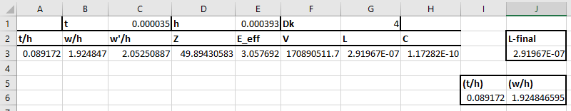
Just as a sanity check, we can quickly calculate the total inductance of a trace determined with this method and compare it with typical values. The inductance of a ~1 in. trace is typically quoted as being 5 to 10 nH. For the optimized trace I’ve designed with this model, the total inductance for a length of 1 in. is 7.4168 nH, which is within the range normally measured for small PCB traces. In addition, if you look at the IPC 2152 nomograph, you can immediately use these results to determine the temperature rise for a given current in this trace.
If you’re interested in getting a copy of this spreadsheet, feel free to email me at zmp@nwengineeringllc.com. The built-in evolutionary optimization algorithm in Excel takes a significant amount of time to converge, although it will give slightly more accurate results than the built-in GRG nonlinear algorithm. One can easily adapt this method for other trace geometries and obtain similar results.
Going Further With 3D Field Solvers for Impedance Control
The best choice for determining trace impedance for a given set of geometric constraints is to use a field solver that operates directly in your layout. If you aren’t familiar with optimization algorithms, you need the right routing tools that contain an integrated field solver for accurate impedance calculations. This type of tool will consider the overall geometry of your board, rather than the isolated trace I’ve considered here. While determining the size of an isolated trace is a great place to start, it does not account for coupling/parasitics in your board. A 3D field solver that is integrated into your interactive routing tools will produce more accurate results for trace impedance and propagation delay.
The routing and impedance calculation tools in Altium Designer® can help you maintain the right PCB trace inductance and widths you need, thanks to the built-in field solver. This set of tools interfaces directly with your routing features and design rules, ensuring you can maintain consistent impedance while satisfying trace width constraints throughout your board. You’ll also have access to a variety of length/delay tuning features for high speed designs.
Now you can download a free trial of Altium Designer and learn more about the industry’s best layout, simulation, and production planning tools. Talk to an Altium expert today to learn more.
