The Increasingly Important Role Of Dielectric Loss Tangent In PCB Laminates
As noted in previous articles, today’s high-speed PCB designs are characterized by two factors: moving lots of data and signal bandwidths spanning up to very high frequencies. As a result, several things influence these two factors. Among those at the top of the list of “if you don’t get this right, you’re dead in the water,” elements are low loss. There are a number of things that are done during the design process that influence loss, but the foundational decision to be made is the dielectric loss tangent of the chosen laminate. In short, the dielectric loss tangent will limit the useful length of a transmission line on a PCB as it causes the signal level to decrease during propagation.
This article will describe dielectric loss tangent, the role it plays in high-speed designs, how it depends on the glass to resin ratio and frequency, how to measure it, and the impact in today’s products. For boards that run at 32 Gbps, we'll look at why building a test board becomes an imperative for qualifying loss tangent.
What is Dielectric Loss Tangent?
Dielectric loss tangent is sometimes called a dissipation factor and is given the symbol Df. In transmission line design and RF design, dielectric loss tangent is defined with the tan(𝛿), which is a measure of the rate at which energy carried by the electromagnetic field (RF) traveling through a dielectric is absorbed by that dielectric. When a material is referred to as "high speed," it is the Df value that is being referenced. Some salient points to keep in mind include:
- At frequencies used in PCBs and microwave components, the amount of energy absorbed by the dielectric generally increases with frequency until you get into the high GHz range.
- Loss gets larger with frequency because the changing EM field causes the molecules in the dielectric to vibrate. The faster they vibrate, the more the loss (more about this below).
- The lower a material’s loss tangent, the lower the power loss.
The dielectric loss tangent of any material has a simple equation in terms of the dielectric constant of that material:
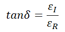
If you know the imaginary and real parts of the dielectric constant, you can calculate the loss tangent. If you look at PCB laminate datasheets, you'll generally see a dielectric loss tangent value and a Dk value. Just multiply these together and you get the imaginary part of the dielectric constant.
It’s All Molecular
The loss in dielectrics at frequencies used in PCBs is caused by the fact that molecules are formed from opposite electric charges, which can attract and repel each other. If an atom in a molecule is displaced from equilibrium by an electric field, it can begin oscillating. All materials will have some loss tangent, even if it is very small at frequencies used in most PCBs.
As an example, consider water, which has some polarity and a non-symmetric structure. There are one oxygen atom and two hydrogen atoms that form a V shape with the oxygen atom at the negative end and the hydrogen atom at the positive end. When a water molecule is subjected to a changing electric field, it vibrates. Note that molecular kinetic energy is directly associated with temperature, so the molecular vibration induced by a propagating field leads to higher temperature in the substrate. This is why microwave ovens work; the water in your food reaches a high temperature as its vibration is driven by an electric field. Molecules can have higher dielectric loss tangent than non-polar molecules due to greater charge separation in different regions of a polar molecule.
The information in Table 1 shows that most of the materials used to make multilayer PCBs have a relatively high loss. (To be classified as low loss the loss tangent should be below .004.)
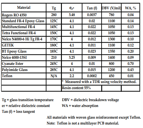
The challenge for PCB designers comes in deciding when one material has too much loss and must be replaced with a lower loss alternative. Since loss is a function of both frequency and the length of the transmission line, there is no easy rule that can be followed to determine when a switch must be made.
Dielectric Loss Tangent, Frequency, and Glass to Resin Ratios
A given PCB laminate is made up of a resin system and woven glass reinforcement cloth, each of which has a different loss tangent value. Thus, as varying ratios of glass and resin are used to create PCB laminates with various thicknesses, the overall loss tangent will vary. This presents a problem for signal integrity engineers when they are supplied only a single loss tangent value for a family of laminates, as is the case with Panasonic and their Megtron 6 material system. Table 2 shows how loss tangent varies with frequency and the glass to resin ratio. This is data for Isola Corporation’s FR408HR core material.
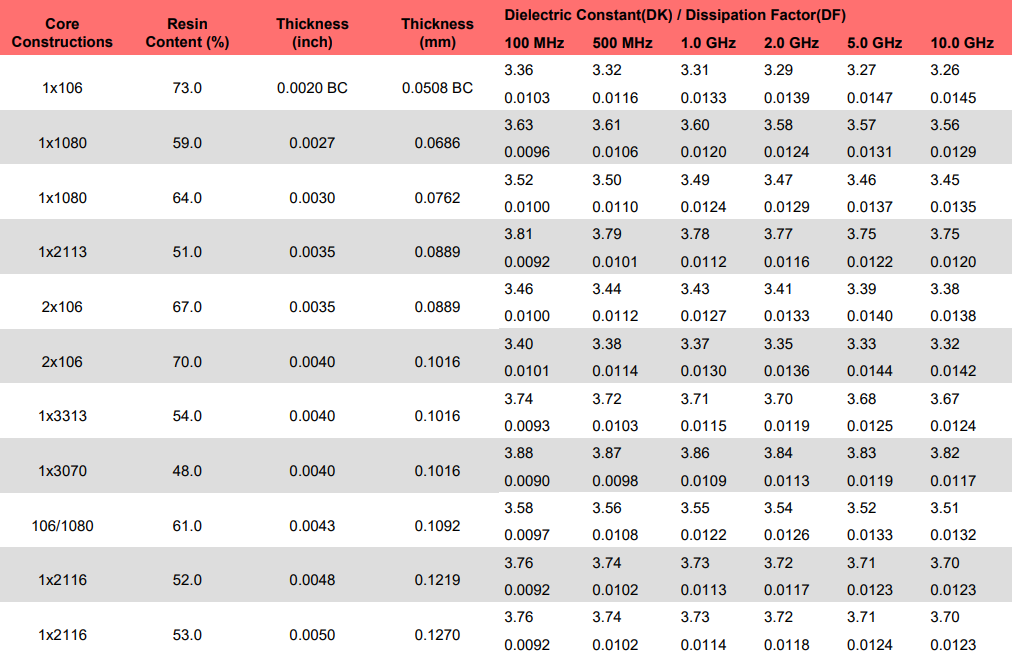
This table contains an example of a well-characterized PCB laminate system. As can be seen, the dielectric loss tangent increases with the frequency more than it varies with glass to resin ratio. This is because, in this system, the loss tangent of the resin system and glass are very close to each other. In other resin systems, this may be different.
Measuring Dielectric Loss Tangent in Digital Laminates
Reference 2 at the end of this article shows that there are 23 different methods documented by the IPC for measuring dielectric loss tangent in laminates. Each of these methods was developed for a particular application. Since the first applications requiring low loss laminates were microwave and RF, most of these test methods have been optimized for a particular type of circuit such as phased array radar. Compared to the demands of very high-speed digital circuits, these applications can be considered “narrowband”.
Only one of these methods characterizes laminate in a manner that is useful in the design of digital multilayer PCBs. This is the Bereskin Stripline method which uses a stripline transmission line to measure loss. It has been demonstrated to correlate best with actual tests performed on PCBs constructed with stripline transmission lines. All of the other methods use resonant cavities or other types of measurement cells that characterize laminates over a narrow range of frequencies, and they all have some errors. The data in Table 2 was obtained using the Bereskin Stripline method.
What To Do When Dielectric Loss Tangent Data is Incomplete?
The typical laminate datasheet does not contain enough information about dielectric loss to allow proper modeling and analysis of potential losses in high-speed digital data paths. How, then, is it possible to ensure a design will work to specifications when it is finally built? This is a question that arises everywhere engineers are developing products that use the latest high-speed data links. It can be further complicated by the need to accurately account for the losses in copper traces, which are affected by the overall surface area of the traces as well as the roughness of the copper surface.
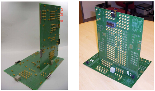
There is no reliable method for modeling all of these effects, even when the loss tangent is accurately known. Therefore, a product developer has little choice but to construct test PCBs with the actual transmission lines to be used in the final product and perform tests to determine the loss vs. frequency for the laminate being considered and see if the goals can be met. This is the only safe method of constructing a design rule set for a high-performance system. Figure 1 is a photo of two actual test PCBs set that we used some years back to validate the paths in a supercomputer that were 5.2 Gb/S and the paths in a terabit router that was 4.8 Gb/S. These test PCBs were designed such that when plugged together, they would create daughterboard/backplane interfaces as well as interfaces that traveled off the backplane and daughter boards to the outside world.
So What About Designing for Today’s 32 Gb/S and 56 Gb/S Data Paths?
It probably comes as no surprise that, when you are designing products with 32 Gb/S or 56 Gb/S data paths, you have to build test boards to make sure your product will work as designed. Lee Ritchey, Founder and President of Speeding Edge, notes: “Once you get to these data paths, loss tangent becomes of even greater concern. You build test boards similar to those noted above. You just measure farther out in frequency. These data rates dominate the performance of the product, and they determine how long of a path you can have on the board. The equation is pretty straight forward, the longer the path, the more loss there is.”
There is an ascending order of the cost of technology that applies to very fast data paths. Copper traces on the board are the least expensive; Twinax is the next step up, and the last step with today’s technologies is fiber optics. Ritchey notes, “A few years back; we did a supercomputer where we had four meters of Twinax under the floor to get from rack to rack. That’s the step that you take before you have to go fiber. Launching through a connector and Twinax at both ends is a lot more expensive than a trace on a board. And, going to fiber is a lot more expensive than Twinax.”
“In ‘big boxes,’ it’s been common to have a path that is 28” long. At 32 Gb/S and 56 Gb/S, that puts you up against the limit,” Ritchey continues. “Compare this to the loss in fiber channels which is two or three orders of magnitude less. For the same frequency, you can run 100 Km instead of 24 inches. Now, in the big boxes, the paths are too long even for Twinax, so people are having to move to fiber. When there is a box-to-box connection or a section-to section space on a big machine, such as that used to scan semiconductors, there are lots of places where fiber has to be used. That’s painfully expensive because you have to have a transceiver, priced at $50 apiece, at each end of the path. So, the incentive is to stay in copper. In 10 Gb/S server farms we improved the transceivers so that we could do 10 Gb/S over Category 6 cable for 100 feet. But going from 10 Gb/S to 56 Gb/S is a giant leap. The really good transceivers can only handle about 30 inches.”
He concludes, “Some vendors are honest about their loss tangents. Others optimistically misrepresent their data because no one checks it. I tend not to trust most of the laminate vendors’ data, so that’s why, if there is a lot of money involved, I build a test board with the real circuit to find out if what we want to do is possible. Bottom line–every time you move up a step in technology, you have to build test boards. There are some good modelling tools, but if the data is bad, it becomes a garbage in/garbage out proposition. There is nothing worse than getting a prototype that won’t work. You have to go back to square one because you can’t fix it. This means your product development costs go up, your scheduled product delivery date is slipped, and you may miss critical market windows. It’s lost time, lost opportunity and, potentially, lost revenue.”
Summary
As the frequency and data rates of today’s PCB circuits have increased, so has the need for accurate loss tangent information of the various types of laminates along with how that loss changes with varying thicknesses. At 32 Gb/S and 56 Gb/S data rates, loss tangent plays an even more significant role in the final operation of the product. At the same time, laminate vendors may supply loss tangent data for their materials. The only way to know if your product is going to work as specified and as designed is to build a test board with the actual transmission lines that will be used in the final product.
Have more questions? Call an expert at Altium.
References:
- “Right the First Time, A Practical Handbook on High Speed PCB and System Design, Volumes 1 & 2,” Ritchey, Lee W. Speeding Edge, 2003 and 2006 respectively.
- “Signal Integrity Simplified,” Bogatin, Eric, Prentice Hall, 2004.
- “An Update on Low Loss Laminates for Use in High Speed Digital Designs,” Ritchey, Lee W. Speeding Edge,
- Current Source Newsletter, Volume 3, Issue 2, June 5, 2009.Loss Tangent Measurement Methods,” Hinkley, Kevin, etal, DesignCon 2010, 5-TP2.
- “Making Sense of Laminate Dielectric Properties,” Pangier, Rich, etal, Isola, December 1, 2008.
- “Dielectric Loss Test Methods,” Novak, Istvan, etal, DesignCon 2010, TP-M2.
- “Materials Characterization Methods,” Khilkevich, Victor, etal, DesignCon 2010, 5-TP1.
- “Right the First Time, A Practical Handbook on High Speed PCB and System Design, Volumes 1 & 2,” Ritchey, Lee W. Speeding Edge, 2003 and 2006 respectively. “Signal Integrity Simplified,” Bogatin, Eric, Prentice Hall, 2004.
- “An Update on Low Loss Laminates for Use in High Speed Digital Designs,” Ritchey, Lee W. Speeding Edge, Current Source Newsletter, Volume 3, Issue 2, June 5, 2009.
- “Loss Tangent Measurement Methods,” Hinkley, Kevin, etal, DesignCon 2010, 5-TP2.
- “Making Sense of Laminate Dielectric Properties,” Pangier, Rich, etal, Isola, December 1, 2008.
- “Dielectric Loss Test Methods,” Novak, Istvan, etal, DesignCon 2010, TP-M2.
- “Materials Characterization Methods,” Khilkevich, Victor, etal, DesignCon 2010, 5-TP1.