Analyzing Crosstalk on FIFO and DDR4 Parallel Bus Interfaces

High speed buses, whether single-ended or differential, can experience any number of signal integrity problems. A primary problem created by propagating signals is crosstalk, where a signal superimposes itself on a nearby trace. For parallel nets, this is particularly problematic as it leads to data corruption in severe cases. While you could slow down the rise time of a signal, this may require lowering the data transfer rate and may be unacceptable in some applications.
If you want to identify crosstalk on parallel buses, it can be quite difficult when the bus is quite wide. For an N-bit parallel bus, you would need to run N(N - 1) crosstalk simulations to examine crosstalk between every possible combination of victim and aggressor trace. Once you get to wide bus widths, this becomes very time-consuming without the right set of analysis tools. Typically, you only need to extract the peak crosstalk signal and compare it to your signalling specs.
The industry-standard PCB design tools in Altium Designer® already include a post-layout simulator for examining crosstalk. Still, you can speed up crosstalk analysis in parallel buses when you use a powerful field solver. You can expedite crosstalk analysis on parallel buses and other groups of signals when you import your Altium Designer layout into Ansys SIwave®. When you can conveniently visualize crosstalk between nets in a wide parallel-to-serial interface, you can speed up your analysis and quickly correct errors in your PCB layout.
What Goes into Signal Integrity on Parallel Nets?
In Identifying Near-field EMI in a PCB’s Power Distribution Network and Spotting DDR4 Impedance Violations in High Speed PCB Design, we’ve looked at the Mini PC example project in Altium Designer, and we examined near-field EMI due to a poorly-planned return path and impedance variations on DDR4 nets. As the DDR4 nets form a parallel bus (containing both differential and single-ended signals), there is also the potential for crosstalk on these nets. Another wide parallel bus with potential for cross talk between specific layers is a 32-bit wide bus routed to a FIFO-to-USB interface.
As these groups of parallel nets form wide buses, analyzing crosstalk on every signal and extracting a peak-to-peak induced crosstalk voltage can be very time-consuming. You can certainly do this by looking at waveforms, but who wants to pick signal values off of waveforms all day?
Instead, crosstalk on these nets can be extracted directly using the field solvers in the Crosstalk Scanner in Ansys SIwave. After your layout is finished in Altium Designer, the Ansys EDB Exporter extension can be used to transfer the design into SIwave and run simulations directly from the PCB layout data. Some of the other important signal integrity metrics that can be examined include:
- Impedance variations on single-ended and different nets
- Return paths for high speed signals
- S, Y, and Z-parameter extraction on critical nets
- Parasitic extraction on critical nets
In this example, we’ll start by looking at single-ended crosstalk on the FIFO nets, followed by the DDR4 nets. As we’ll soon see, Ansys SIwave provides a convenient visualization that allows the victim/aggressor net pair to be identified. A potential solution for the net pair can be implemented, and the modified net can be analyzed in more detail using the post-layout simulation tools in Altium Designer.
FIFO-to-USB Nets
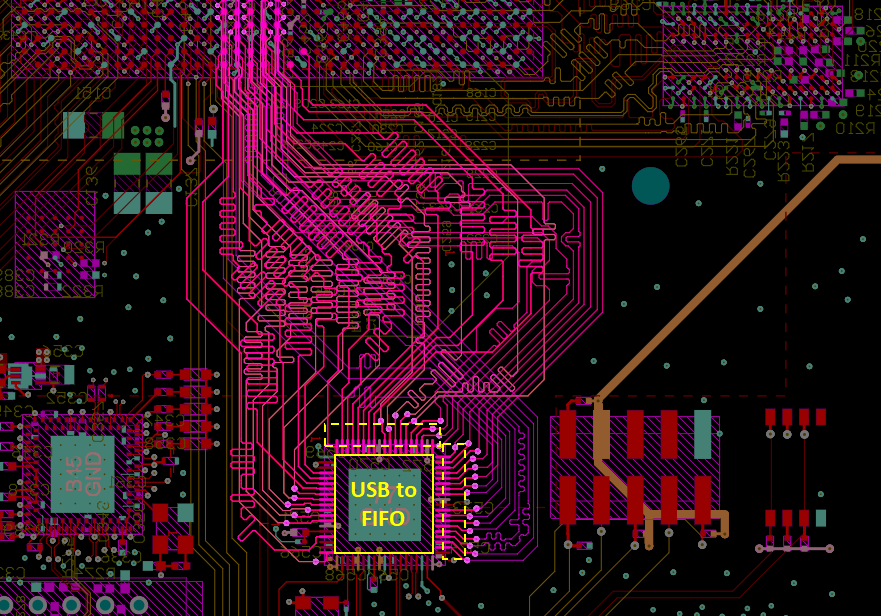
Figure 1 shows the highlighted FIFO nets on Layers 1, 5, and 7. These nets form a 32-bit wide parallel bus with single-ended source-synchronous clocking that connect to a FIFO-to-USB interface IC (U33 in the Mini PC project). Length matching has been enforced to prevent skew between the synchronous clock and the 32-bit data lines in this bus. The nets in these layers are separated by large ground planes on the intervening layers.
DDR4 Nets
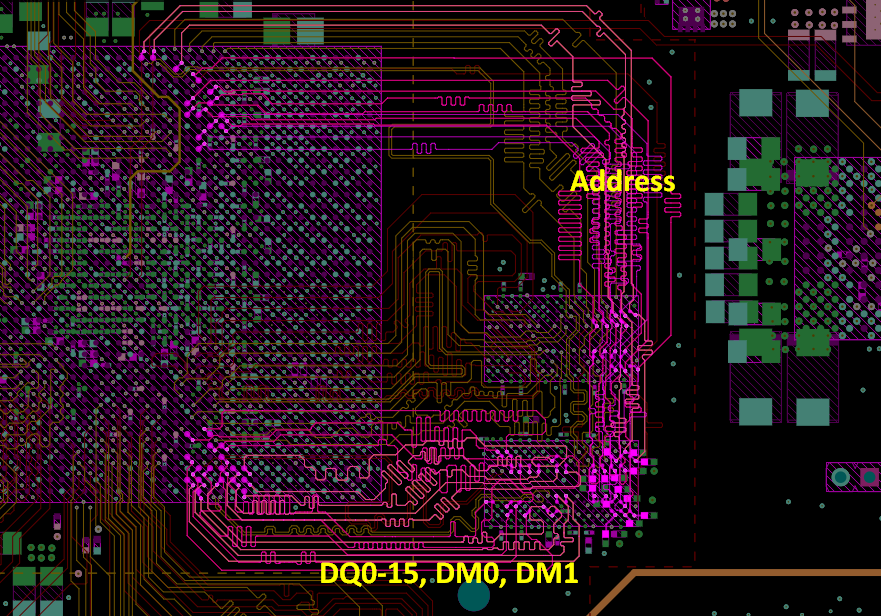
The Mini PC board contains two onboard 8 GB DDR4 DRAM chips running at 1866 MHz routed in fly-by topology. Byte lanes 0 and 1 are grouped together with tight routing and length matching in one area of the board, while the address lines are routed around the edge of the DDR4 modules in the typical fly-by topology. Here, we basically have two parallel buses to simulate: the address lines and the DQ/DM lines leading to each module. Figure 2 shows the address, DQ, and DM lines that will be examined in the Mini PC layout.
Crosstalk Scanner Results
After running the Crosstalk Scanner in SIwave for the parallel buses shown above, we can see precisely which net pairs exhibit the greatest crosstalk signal (NEXT and FEXT). This tool uses an idealized stimulus signal that matches the rise/fall time for the FPGA in this board. The peak-to-peak voltage can be shown in a 3D bar graph, where the net names are placed on the x and y axes to form a symmetric square matrix. The FEXT and NEXT crosstalk signals produced by a given net pair can also be visualized in the time-domain.
Figure 3 shows the peak-to-peak crosstalk (NEXT) for the FIFO nets shown in Figure 1; only a subset of the FIFO nets leading to the FIFO-to-USB IC are shown for clarity. The peak-to-peak voltage for the induced crosstalk signal is quite large and reaches 100 mV or 8.33% of the nominal single-ended signal level (1.2 V) on these nets. This indicates relatively low isolation, particularly between the clock signal (USB3_CLK) and some nearby data nets (strongest NEXT seen USB3_D10).
The bottom portion of Figure 3 shows the extracted crosstalk signal from USB3_D2 to USB3_D3 in the time domain. Here, we see that the FEXT signal is quite low and only reaches ~10 mV (-21 dB). In contrast, NEXT is relatively high and reaches ~100 mV.
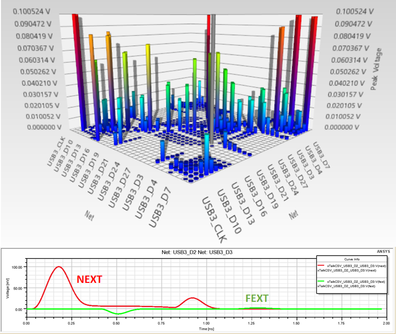
Figure 4 shows the peak-to-peak crosstalk (NEXT) for the DDR4 nets shown in Figure 2; only a subset of the nets in Figure 2 are shown for clarity. The peak-to-peak voltage for the induced crosstalk signal does not exceed 7.5 mV, or 0.625% of the nominal common-mode signal level on these single-ended nets. This equates to minimum of -22 dB isolation between address nets, which is sufficient for high-performance memory systems. The other nets in the DQ/DM section have much higher isolation. Finally, the address and DQ/DM sections are clearly separated by enough space that crosstalk is not problematic.
.png)
Because the Mini PC board is a linear time-invariant (LTI) system and the electromagnetic field does not pass through any biased nonlinear media, one would reasonably expect the system to be reciprocal, i.e., the crosstalk signal will be the same if the victim and aggressor nets are swapped. This can indeed be seen in the crosstalk results for the FIFO nets and the DDR4 nets. Because the DDR4 bus falls within the crosstalk limits found in high-performance memory systems, we can focus on potential modifications to the FIFO bus.
Reducing Crosstalk on the FIFO Bus
When we inspect the FIFO layout and the NEXT results, it is clear inductive crosstalk dominates in the traces in this bus. Therefore, the natural solution, in this case, is to decrease the inductance of these traces by making them wider or by bringing them closer to their reference plane. The latter option is impractical in a completed layout, especially considering the solutions proposed in our earlier blogs in this series.
Although changing the stackup is insufficient, there is sufficient room on Layers 1, 5, and 7 to widen the traces. Spacing between traces should be maintained to prevent an increase in mutual capacitance as these traces are spread out. If we look at Figure 1, the FIFO bus should be spread out towards the right side of the image. Length matching will need to be enforced as modifications are applied to traces in the FIFO bus.
Summary
Crosstalk on parallel bus interfaces Altium Designer’s Mini PC example project was examined using the Crosstalk Scanner in Ansys SIwave. Specific nets in FIFO and DDR4 buses were identified for modification using a convenient crosstalk visualization, which summarizes induced crosstalk signals for pairs of aggressor and victim nets. Furthermore, the dominant crosstalk mechanism (inductive vs. capacitive) can be identified from looking at time-domain waveforms, which then helps determine some solution to implement in Altium Designer.
Register for the joint Altium and Ansys webinar to learn more.
By using the Ansys EDB Exporter extension in Altium Designer®, PCB designers can transfer their PCB layout into Ansys SIwave® and run multiple signal integrity and power integrity simulations. This simulation package takes data directly from your PCB layout and gives designers access to numerous 3D field solvers for time domain or frequency domain simulations and analyses.
