Power Integrity Analysis in Your PCB Design Software
Power integrity problems can abound in modern PCBs, especially high speed boards that run with fast edge rates. These systems require precise design of the PDN impedance to ensure stable power is always delivered throughout the system. Without carefully considering the PDN characteristic impedance, you’re at risk of creating ripple and noise in the power distribution network when fast signals switch states.
Some designers might wonder what is power integrity analysis: it’s a set of methods for understanding how your components draw power and how the structure of the board affects stable power. The power integrity analysis process in circuit board design is much simpler when you use an application like Altium Designer. With an integrated toolset and connectors to external applications, you can identify and solve many common power integrity issues.
ALTIUM DESIGNER
A unified PCB design application with a full suite of controlled impedance routing features for professional designers.
Professional designs that operate a high voltage, high speed, high current, or high frequency can experience a range of signal integrity and power integrity problems during operation. There is a range of signal integrity problems that begin as power integrity problems, and these need to be addressed early in the design phase. Power integrity analysis aims to identify many problems with power delivery in a circuit board, which can later cause signal integrity problems.
To solve common power integrity problems, it’s important that designers have the best set of analysis tools to calculate and solve power integrity problems in a finished circuit board layout. Altium Designer includes these important power integrity tools and many more to help you stay productive as you create high-quality PCBs.
Solve the Most Common Power Integrity Issues
Every circuit board will have some common power integrity problems that need to be identified by examining the PDN. The PDN impedance, S-parameters, Z-parameters, DC current density, and voltages are all important points to examine and calculate as part of power integrity analysis of an electronic system. In some systems, power integrity problems are minor and may not be noticed in measurements. However, in high speed PCBs with fast signal edge rates, many common power integrity issues can be observed and can lead to system failure.
Some of the common power integrity problems that can occur in a circuit board include:
- High PDN AC impedance and/or DC resistance
- Power rail collapse and ground bounce
- Radiated emissions due to weak decoupling
- Excessive heat generation
- ESD at high voltage
The DC resistance in a circuit board depends on the dimensions of your power plane and interconnects, and it’s the starting point for understanding power integrity. Once this aspect of a circuit board is addressed, a designer can take steps to ensure they meet target impedance goals to prevent signal integrity problems that arise from unstable power delivery.
Solve Common DC Power Integrity Impedance Calculations
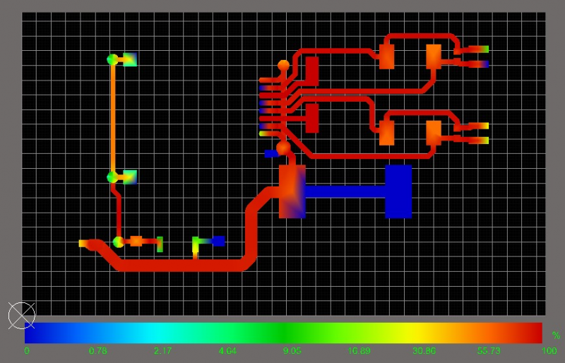
With DC resistance, current density, and voltage distribution being so important for power integrity, designers need analysis tools like the PDN Analyzer in Altium Designer. This simulation engine is built to perform DC power integrity calculations directly from your PCB layout. You can then identify areas of a board where there is excessive current and heat generation before a prototyping run.
- Make sure you understand what factors contribute to PDN resistance and total impedance.
Learn more about PDN inductance and how capacitance affects power integrity.
- When designing a PCB power plane, be sure to first calculate the current carrying capacity for your PDN and ensure your design has the required DC resistance.
Learn more about calculating current density limits for power planes.
- A DC power integrity calculator will show you the DC resistance, current density, and voltage distribution throughout your power planes and power delivery subsystem.
Learn more about using a PDN analyzer utility for DC power integrity analysis in Altium Designer.

Easily calculate and track DC current density in your power delivery network.
Power Integrity Analysis for High Speed Design
High speed PCBs rely on exact transmission line impedance to ensure the design will operate correctly, but they also require very low power delivery network impedance. Circuit boards for high speed digital systems are designed with a target impedance in mind. The PCB stackup, selected decoupling capacitors, and PCB laminate thickness combine to determine the impedance of the PDN, which is intended to be designed to meet a target impedance spectrum.
Keeping the PDN impedance low is important for ensuring high speed components do not create power rail ripple and ground bounce when they switch. If the PDN impedance is low enough, then these effects will not be noticed in the system. Once the plane impedance in the PDN has been calculated, it’s now possible to determine whether any power rail ripple and noise will cause the power delivery to fall outside allowed limits.
Design the Best PCB Stackup for Low PDN Impedance in Altium Designer
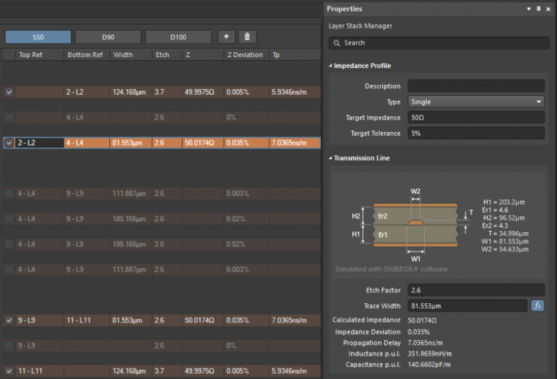
Designing to low PDN impedance requires placing ground and power layers close together on adjacent layers to ensure high plane capacitance. It also helps to select the right set of PCB materials to ensure the design has low loss and low PDN impedance. The integrated Layer Stack Manager in Altium Designer is the first tool you’ll use to ensure you’re designing to your target PDN impedance as you create your design.
- Once you’ve received your prototype boards for your design, it’s important to measure power integrity to ensure you’ve hit your target impedance goals.
Learn more about PDN impedance measurements and power integrity.
- S-parameter models and Z-parameters are two mathematical tools you can use to perform power integrity analysis and ensure you’ll reach target PDN impedance.
Learn more about network parameters for power integrity analysis.
- Altium Designer connects to Ansys SIwave to help you identify and solve impedance and EMI problems in high speed PCB designs.
Learn more about using field solvers for power integrity analysis.

High speed PCB design and routing starts with creating a PCB stackup that enables impedance control.
Finish Your High-Performance Board with Altium Designer
Altium Designer includes a complete set of integrated design tools to help you place and route all the components you need for your high speed design. In addition to your impedance and DC analysis features, you’ll have a set of simulation tools to help you evaluate your PCB layout and identify potential signal integrity and power integrity problems in your circuit board layout. When you’ve finished your design, it’s time to prepare it for fabrication and assembly, and Altium Designer will be there to help you finish the job.
Take Your Design to Fabrication and Assembly
Altium Designer helps you complete your design projects successfully by instantly preparing your board for manufacturing directly from your design data. You can export all your design files as fabrication and assembly data without using any external application. You’ll also have an integrated tool set for managing your PCB design and manufacturing data with the Altium 365 platform. Everything you need for high speed/high frequency design is accessible in a single program with Altium Designer.
- Everything you need for design, manufacturing, layout, routing, and simulation is included in Altium Designer.
Learn more about the unified design environment in Altium Designer.
- The integrated PDN Analyzer utility interfaces directly with the Layer Stack Manager in Altium Designer, giving designers an integrated tool for accurate DC analysis.
Learn more about the PDN Analyzer utility in Altium Designer.
- When you’re ready to share your project with other PCB designers or your manufacturer, Altium 365 lets you instantly share your circuit board design and production data through Altium Designer or on the web.
Learn more about sharing your PCB project data with Altium 365.

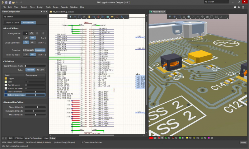
Layout your impedance controlled high speed PCB design with ease in Altium Designer.
Don’t settle for external PDN impedance calculators and capacitance optimization tools, stay productive and create the most accurate designs in a single program with Altium Designer. No other design application includes a full suite of design features for high speed design with integrated power integrity analysis tools.
Altium Designer on Altium 365 delivers unprecedented integration to the electronics industry until now relegated to the world of software development, allowing designers to work from home and reach unprecedented levels of efficiency.
We have only scratched the surface of what is possible to do with Altium Designer on Altium 365. You can check theproduct page for a more in-depth feature description or one of theOn-Demand Webinars.
