PDN Analyzer Simulation of 65W Single IC LED Driver
In my last article, I designed a 65W LED driver for powering a 36V LED string at 1.8A. The small MSOP-8 IC on it is going to get quite warm, which makes me believe the power distribution network is worth simulating with PDN Analyzer. This will allow me to see if there are any spots that need optimization on the board.
Anywhere I can reduce the current density in high-current areas to ensure a lower copper temperature will be worth the time investment. In addition, I want to make sure the voltage drop is not going to be excessive anywhere on the board, which could cause functionality issues in the design.
I’m going to do a full simulation of the board, with both switched-mode power supplies being modeled in the network as loads. By modeling the full network, I will have the most complete overview of current and voltage on the circuit board, which will allow for a thorough analysis of the design.
If you missed the previous article and would like to see how the LED driver was designed, you can find it here. If you just want to see how to configure PDN Analyzer for a simple project with multiple switched-mode power supplies, you can download the Altium project from GitHub. Like my other projects, this project is open source and free for you to use.
PDN Analyzer is a simulation tool for Altium Design that I find incredibly useful; it saves board revisions and troubleshooting due to design deficiencies that could have been caught prior to ordering boards.
Set Up Nets
The first step of any PDN Analyzer project is to set the nets up. I like to set up as many nets as possible when first starting the project, so I don’t need to come back to add anything later.
Set the nominal voltage on any net that you will be adding to the simulation. I find it’s worth having a PDF copy of the schematics open on screen, or a printout of them, when setting up PDN Analyzer nets and the simulation in general. The DC Net Identification window doesn’t allow you to use the Altium schematic viewer window while you’re setting up the nets, so having a copy outside the software is handy and can save time. This is particularly useful if you forgot to add a name to a net that you want to simulate, such as my NetD3_1 and NetIC1_1 in the screenshot above. Without having a copy of the schematic, I might not have realized that these nets do need simulation!
Configuring the First Net
I like to work my way from the input power connector to the output connectors when setting up PDN Analyzer. If I have a complicated schematic to simulate, a printed copy allows me to highlight or cross out what I’ve completed, thus ensuring I don’t miss anything.
My input is reverse polarity protected with a MOSFET, so I’ll start with VIN and CN_GND rather than VIN and GND. This will allow me to simulate all the way back to the input connector and verify the current through the MOSFET is within its limits. You can set the net by double clicking on <Power Net> and <Ground Net> and selecting the relevant DC net, in this case, VIN and CN_GND.
Next, we’re going to configure the voltage source by right-clicking anywhere and selecting Add Source.
In the Device Properties window opened by clicking Add Source, you can set the Device Type to Voltage Source, and then select the reference designator of your input connector component, which in my case is J1. The pins should automatically populate for you. If they do not, you have likely selected the wrong component as the PDN Analyzer could not find a pin that connects to the net you selected.
This will then show the source on the left side of your network.
Extending the Network
Now that we have the basics of the first network created, we’re going to need a way to tell PDN analyzer that there is a connection from GND to CN_GND through our reverse polarity MOSFET. You can right-click on CN_GND and choose Extend Net.
This will then let you choose a net that you can extend to, which, in this case, only has the one option of GND.
This will then create a join that can be configured by double-clicking. The join will have a device type of Series Element that cannot be changed. Select the reference designator of the component that is going to join the nets. This MOSFET has an RDS(on) of 116 milliohms, so you can set that in the parameters. It also has a maximum current of 2.7A, so I’m going to set that as well. If I exceed this current, PDN Analyzer will let me know, and I will consequently choose another MOSFET for my reverse polarity protection that has a higher current rating.
This is a feature of PDN Analyzer I really like, as sometimes I get so caught up in the high power circuits that I forget to add up the current of all the smaller loads when calculating a component’s maximum capacity requirements. PDN Analyzer adds a nice sanity check to my design, saving me from headaches during prototyping, or worse, production!
Simulating Resistive Dividers
Another great reason for extending a net is to calculate resistive dividers. By adding an extension for the top leg of your divider, and a load for the bottom leg, you can visualise voltage drops across the copper. If your divider is a long way from where it is referenced, the resistance of the circuit board traces could drop your voltage to a potential that is lower than you require.
The MOSFET I’m using for reverse polarity protection has a maximum gate voltage of 14 volts, a lot lower than my input voltage of 48 volts. Therefore, I have a resistive divider on the gate to provide me with a potential that is low enough across the entire expected input voltage range so as not to burn out the gate.
We start by simulating the reverse polarity protection and setting up basic nets.
Once the VIN net is extended, we can set the extension element to be a 33k resistor, then add a load to the net by right-clicking and selecting Add Load.
Next, we need to set the Device Type to Resistor. If I haven’t used PDN analyzer in a while, I usually forget to set the device type and leave it as IC (Current), which confuses the heck out of me later when I do the simulations.
Then, we just need to select the reference designator of the resistor that acts as the bottom leg of the divider, and set its resistance value.
The input group is now complete, and we can continue setting up the rest of the power network simulation.
Our simulation for the input group now has a source, a load, multiple resistive connections, and multiple nets
Adding the 12V Switched Mode Regulator Simulation
We now need to simulate the 12V Switched Mode Regulator.
Our simulation starts with extending the VIN network across the ferrite bead, FB2. The ferrite bead has a 150 milliohm DC resistance, which we set on the series element.
Following that, we can right-click on NetC13_2 and add a load. This time, we’ll set the device type to VRM (SMPS), then configure out the input and output reference designators. I already calculated the efficiency of the regulator during the schematic design phase, so I can enter that into the parameters as well as the output voltage.
Now that the voltage regulator is in the simulation network, we can configure the loads for it. To do this, we’ll need to create a new network for the voltage regulator. This can be done by right-clicking on the VRM load and selecting Add VRM to New Network.
In the simulation list, you will now have the new 12V net, which you can select for adding the loads.
The first loads are easy, the 40mm 12V fans that I was considering for this project were all typically around 150mA of max current draw. To simulate these, it’s just a matter of adding a load for each of the connectors J4, J5, and J6.
There are also several other requirements for the 12V network. I want to simulate the feedback pin and voltage divider to ensure the voltage at the driver is accurate. There’s an LED running off the 12V supply as well, so that too should be added to the simulation. Finally, we are also running the IADJ pin on the LED driver from the 12V regulator, so we need to add the voltage divider for it to the network as well.
That completes the 12V supply network, now we can move onto the main event, the LED driver network.
Simulating the LED Driver
Now, we are ready to add the LED driver itself to the board. This is where the results of the simulation will be most interesting to analyze. I’m particularly interested in seeing the input to the regulator and the ground connection of the exposed pad. The input to the regulator is a single pin in a fairly busy area, so the current density on the board might exceed what I’m hoping for—that also happens to be the area of the board where I need to keep the temperature as low as possible.
Let’s set up the network for the LED driver so we can get on with the analysis!
Finally, we add the LED driver to our simulation
We start, as usual, by extending VIN through the ferrite bead to VIN_DRV.
Then, I’m going to set up the undervoltage lockout divider with the MOSFET next, as I want to check that the voltage on this pin is going to be within the right range. Adding this is just a matter of extending the VIN_DRV network through R4 then through IC3 to the load of R8.
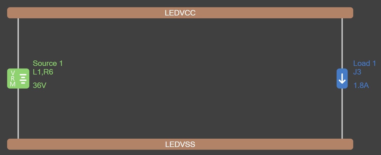
Finally, before adding the LED driver itself, we need to have LEDVSS added to the network, as this will be the output ground for our voltage regulator module in the network. This is just an extension of GND through R6 to LEDVSS.
Now that all our net extensions are complete, we can add a load to VIN_DRV. Again, I have already calculated the efficiency of the driver, so I can enter that into the efficiency field accurately, and I know the output voltage.
This gives us our final VIN network for this section of the schematic. Just as with the 12V regulator, we need to Add VRM to Network on the LED Driver to create a new network that we can add the LED connector load to.
The load is going to be 1.8A on the J3 connector, and that’s the only work required on the LEDVCC/LEDVSS network for us to be able to run the simulation.
Final Simulation Settings
Before we run the simulation, I want to add an upper limit to the conductor currents. There are a couple of spots I’m expecting to see high current density at, primarily around the input to the LED driver pin, and I want to make sure those don’t get too excessive.
To set an overall limit for the board, we can right-click on the simulation and go to Settings.
Then, on the limits settings tab, I can set my maximum current density on a surface layer to 60A/mm2. This is quite high, but I’m hoping the board will be under. I’m also hoping that if it is over, it will only exceed the limit right at the neck of the driver input pin.
With that done, we can now click the Analyze button and see what happens!
Analysing the Simulation
Immediately, we are told that there is a violation in the simulation. Not a great start, but this is what PDN analyzer is for, finding these issues before we get to manufacturing.
To track the violation down, we can look at the network list, and see that VIN has a red exclamation mark next to it indicating that it has a violation or failed check.
Looking in the VIN network, we can see exactly where: right on the VIN_DRV network going to the LED driver.
If you move your mouse over the net that is violating, you’ll see what the error is.
Unfortunately, it looks like what I thought was going to be plenty high for a current density limit was still exceeded. The message tells us where on the board, but we can also find it visually with the Highlight Peak Values tool in PDN Analyzer. When looking for something that is exceeding my requirements, I like to set the color scale to manual and set the maximum to my requirement. This way, anything that is over will be colored black on the board.
Combining the manual color scale and maxima highlight rapidly identifies the issue on the circuit board. The maxima are circled, and anything over 60A/mm2 is very obvious with it’s black color.
The region shown in black is in the copper polygon connected to the VIN_DRV net, and has a very high current density
This area of high current density is not at all what I was expecting. My expectation was that the highest current would be right on the pin! It’s an issue that needs to be fixed, as this current density will cause the copper to heat up in an area of the board at which I’m trying to reduce heat as much as possible.
The only problem is that this section of the board is quite tight with not a lot of room to add additional copper area.
The same region is shown just under the capacitor (brown at the center) in this 3D view.
If I move the input decoupling capacitor next to the pin, right where the high current density is, to the left, I’ll have to move the large capacitor and then in turn the diode. All of which need to be about where they are. So I’ll move over the undervoltage lockout components that are on the right. This will consume some of the ground pour, but the PDIM trace and via are already cutting that area of pour, so it seems like the best option. UVLO is not a sensitive net, so is the most suitable net to move further from the pin.
With the components moved and the polygon pour extended, there’s a lot more conductor area through the section that was having trouble. Now, I can restore the ground polygon and run the simulation again.
It looks like the extra conductor area did the trick. The simulation has now run with no violations showing.
When highlighting the maximum now, we see it is where I was originally expecting the highest current density to be. Just the pin and neck down are highlighted, which is perfect. There’s not much I can do to improve this area, as the pin spacing is my restricting feature.
Using the probe tool I can look at the area that was causing problems in the last simulation. When clicking precislely the same area, I can see the current density has dropped to 19.19A/mm2, which is a fantastic improvement from such a small change. Without PDN Analyzer, I would not have realized this area around the capacitors needed to be expanded.
I can now set the display to a manual color range of 0-50A/mm2 and see what the whole top layer looks like with all nets turned on.
There’s no black areas in the conductors, so the small change has solved the highest current density path.
The ground pour under the LED driver IC is seeing a lot of current density as expected. This appears to drop off quite rapidly as it makes its way out to the groups of vias, which is promising from a thermal perspective. It would be nice if there was a way to open this up further, but the inductor to the north (in the picture above) restricts our options. The current density right on the vias is highest, which I hope will mean that the vias will also conduct a lot of heat away as well as current.
Checking the Resistive Dividers
This example is admittedly a bit contrived, as my voltage dividers are right next to the pin that will be using them, however, it’s a good sanity check even on a board this simple. On a more complex board, this could be a more critical check.
Again, I can use the probe, this time in voltage mode, and hover over the pads I’m interested in.
Hovering over the IADJ pin on the LED driver, it looks like the voltage might actually end up higher than I had calculated by 165mV. I’m not sure if this will be the case in the real board, but it will be worth adding to my physical checklist. It’s about 10% high, which is within reason and the resistor value tolerance will also affect this voltage on a real board.
Finally, I want to check that the UVLO voltage will be over the threshold. This is probably worth running the simulation multiple times, changing the voltage on the VIN source each time to the minimum and maximum I expect to see the board supplied with. This will allow me to quickly check that the pins are going to get the right voltage at both extremes of the input voltage.
With the nominal voltage, UVLO looks great.
Personally, I like the probe tool; it’s great for engineers working on boards to check their design. The tables of data and pass/fail checks are fantastic for overall design verification and for reports to send to a client or management, as well as for my day to day usage. On the other hand, the probe and visual tab tools allow me to quickly verify sections of my design that I may have thought were questionable or needed a sanity check, and are the tools at which I’ll spend most of my time as an engineer. PDN Analyzer’s visualization and probe tools do that much faster than I could do with a spreadsheet of formulas or by calculating copper areas by hand.
Simulation Outcome
After simulating this board, I was able to find a section of copper that was inadequate for the current demands placed on it. By accurately identifying the precise point where the layout was lacking, it was possible to resolve the issue with some very minor tweaks. After revision, the current density in this area which had failed to meet requirements dropped to a third of the original design load. I was able to validate that most of the other current conduction paths on the board were below 10A/mm2, which means that they will contribute very little thermal load to the system from resistive losses.
Using the probe tool, I was able to determine that my resistive dividers will indeed have the voltage I expect from them, which helps both as a sanity check of the values chosen in the schematic design phase, and to ensure no resistances on the board are adding phantom resistive dividers to the network.
If you’d like to try using this 65W LED driver to learn how to use PDN analyzer, you can find it on GitHub released as an open source design. You can download the project prior to the addition of PDN Analyzer, and changes to the board design based on the simulation analysis, at this commit.
Should you wish, you can base your own LED driver on the published design, or build it as is for whatever purposes you design. If you find any issues, you can submit a pull request with corrections.
See more Altium Projects or check more projects by Industry Expert Mark Harris. Have more questions? Call an expert at Altium.