PCB Testing 101: Important Methods and Metrics
Manufacturers know that a lot will go into the PCB fabrication process in terms of quality control and PCB testing. There are many quality checks used to ensure a design will be manufacturable at scale and with high quality, but a lot of this can happen in the background without the designer realizing. Other important tests, like board bring-up and PCB functional testing, are generally the responsibility of a designer during prototyping, and these tests will get wrapped into manufacturing when producing at scale.
No matter what level of testing and inspection you need to perform, it’s important to determine the basic test requirements your design must satisfy and communicate these to your manufacturer. If it’s your first time transitioning from prototyping to high-volume production, read our list of PCB testing requirements so that you’ll know what to expect.
PCB Testing During and After Manufacturing
There are several PCB testing procedures performed during fabrication and assembly. These aim to assess bare PCB quality and yield, and to ensure a design has passed through assembly without defects. In addition, electrical testing will be performed during manufacturing/assembly and compared with the design netlist.
For prototype designs, testing doesn’t end with manufacturing. Once the boards are received, the design team should put everything through board bring-up testing and functional testing before finalizing the design. Once you scale to thousands or millions of boards, some of these measurements may need to be automated to ensure high throughput and quality.
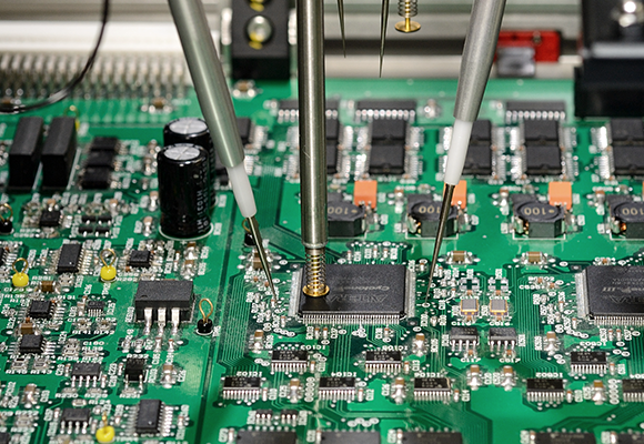
Mechanical PCB Testing and Inspection
There is a minimum set of mechanical tests and inspections that are performed during manufacturing to verify the fabrication process and to ensure the board will be reliably assembled:
|
|
|
|
|
|
|
|
|
|
|
|
|
|
|
|
|
|
|
|
These tests can be used to determine whether there is some quality problem inherent in the manufacturing process, what rework steps might be required, or whether there is some aspect of the design that leads to a failed test. In addition to these basic tests, your board may need to pass through more stringent tests, such as MIL-STD vibration tests, NEMA/NFPA/FAA fire safety tests, thermal shock tests, HALT/HASS tests, burn-in testing, environmental tests, UL safety tests, and other product/industry-specific tests. If your manufacturer cannot perform these more advanced tests, there are specialty testing companies that will qualify new products with a comprehensive methodology.
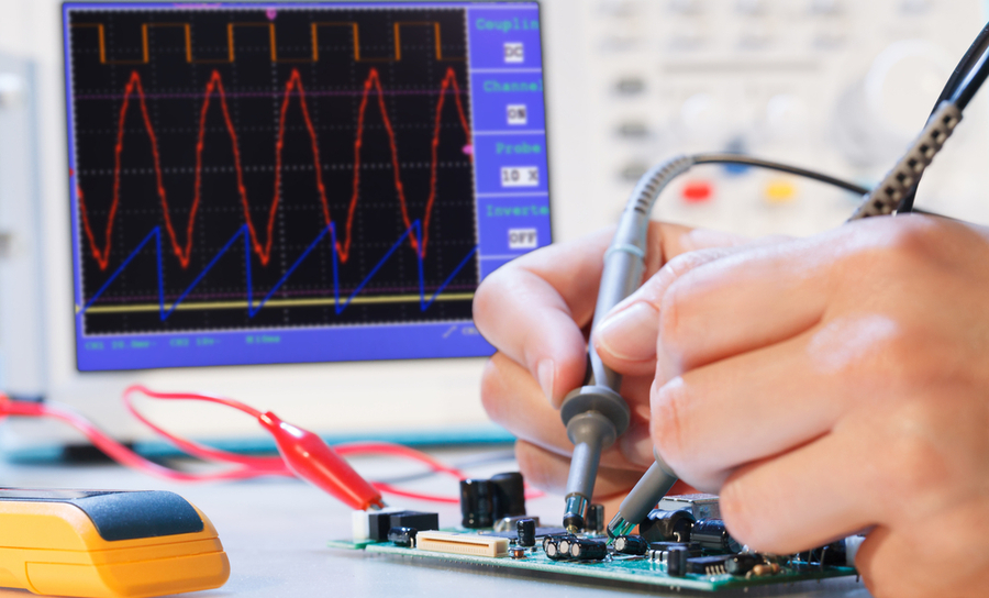
Electrical PCB Testing During Manufacturing
Electrical testing is also performed during manufacturing to check for any faults, impedance deviations, or conductive residues from soldering:
- In-circuit testing: Measures for the presence of opens and shorts, as well as specific voltage/current values on test points. Sometimes a test fixture is used to measure a specific waveform. In addition, power-on or power-off electrical tests may be used with specific components or test points to check for component faults.
- Resistivity of solvent extract (ROSE) test: This conductivity measurement is used to check for any residue that may be leftover from solder flux.
- Time domain reflectometry (TDR): This test is used to measure impedance in single-ended and differential traces. This may be performed on a test coupon or on a test board with an attached fixture. Some subsequent de-embedding and analysis is needed to fully evaluate signal integrity.
PCB Functional Testing
Functional testing for electronics includes a range of possible tests, many of which are focused on ensuring the product provides the desired user experience and end functions that were intended in the design. This is the responsibility of the design team during the prototyping phase, rather than the responsibility of the manufacturer. Remember, your manufacturer’s job is to give you a PCBA that electrically matches the design data you give them, it is not their responsibility to perform functional verification.
In the event the design doesn’t produce the expected functional test results, it’s up to the designer to troubleshoot and debug the design to determine the problem. The designer or test engineer may need to manually gather some electrical measurements, experiment with firmware, and retrace problems through the design to locate the causes of any defects. Once these are located, they can be addressed in the next design revision and, ideally, can be incorporated as test requirements as the product is moved into higher volume.
If you’re making the transition into higher volume, and your product’s functionality or standards conformance requires passing specific electrical, thermal, or mechanical tests, you should specify these for your manufacturer. Talk to them early to make sure they understand what you need and that they have the capabilities to automate these tests to ensure product quality. It takes time up-front to complete these tasks, but you’ll have some piece of mind knowing every possible fault has been anticipated in the design.
The best PCB design tools in Altium Designer® give you everything needed to define PCB testing requirements in your schematics and as attached documents. When you’re ready to send your design our for manufacturing, you can easily release your design data to your manufacturer with the Altium 365™ platform. Altium 365 and Altium Designer give you everything you need to pass a design review, communicate test requirements, and communicate design changes.
We have only scratched the surface of what’s possible with Altium Designer on Altium 365. Start your free trial of Altium Designer + Altium 365 today.
