How 2x Thru De-embedding is Used in Interconnect Characterization

Whether you’re just getting acquainted with high bandwidth interconnect characterization or you’re getting familiar with the new IEEE P370 standard, 2x thru de-embedding will likely become a greater part of daily life for signal integrity engineers. The 2x thru structure is a standard test structure for interfacing between test connectors and a DUT for VAN measurements with the goal of extracting S-parameters or impedance measurements from high-speed interconnects.
Whether you’re trying to build a library of standardized S-parameter data or you need to get some consistent data for your design, 2x thru de-embedding gets you back to data for your DUT. There are a few ways 2x thru de-embedding can be used as part of a larger design process for broadband interconnects and for determining signal integrity metrics generally. In this article, my hope is to introduce newer designers to the concepts behind this and other test structures, as well as some methods for de-embedding S-parameters from a 2x thru structure.
What is De-embedding?
First, a bit of background; If you’re working with high speed signals that have fast edge rates, the relevant signal bandwidth can easily extend beyond 50 GHz, which exceeds the range to be addressed by the new IEEE P370 standard. Newer designs are pushing edge rates higher (easily into ~100 GHz territory), and standards like USB 4 explicitly place limits on broadband signal integrity metrics, not just at one frequency. Therefore, getting accurate measurements throughout the relevant signal bandwidth is critical for design evaluation.
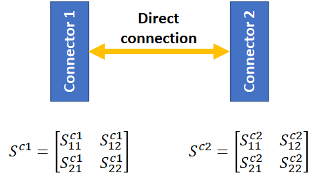
Enter de-embedding, which addresses the test and measurement side of your design. There are already field solver utilities to address the simulation side. Still, the measurement end can be used to determine appropriate stackup and trace geometry conditions to ensure consistent impedance with low loss. To get these measurements, we want to have only the network parameters for the interconnect (normally just S-parameters). A typical test network for a single-ended line is shown below (note; this can be easily extended to a differential line).

The challenge here is that you cannot merely divide out the connector S-parameter matrices to get the transmission line S-parameters, because S-parameters for cascaded networks are not formed by multiplication. Therefore, if you want to measure anything about a transmission line on a test coupon, you have to remove the influence of the connectors or probe interface used to take your measurements.
The central idea behind 2x thru de-embedding is to address the fact that a transmission line will form a cascaded network with whatever is connected at its ends. A 2x thru structure removes the transmission line and uses a direct connection between the two connector ends.

Note that a Beatty standard is specified in place of the transmission line under IEEE P370 to determine the 2x thru S-parameters. With the measurement of the 2x thru S-parameters, we can now perform de-embedding.
How to Do 2x Thru De-embedding Properly
Suppose you have a test transmission line that you’ve simulated with a field solver or an impedance calculator. The result of de-embedding is data that reflects your test transmission line. De-embedding is not limited to 2x thru structures; it’s used generally to characterize any test structure that interfaces to an interconnect.
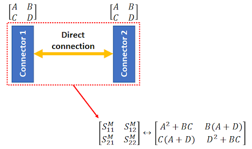
To do 2x thru de-embedding correctly, you have to get the S-parameters of just the left or right interface. This is because the 2x thru structure gives you the S-parameters of the combined network, not of each side of the 2x thru. Some commercial tools can help you to perform this de-embedding, such as Amphenol’s AICC De-embedding Utility.
If you have MATLAB, you can use the s2abcd() and abcd2s() functions to convert between ABCD parameters and S-parameters for the 2x through network. There is an intermediate step where you have to solve four simultaneous equations to get the ABCD parameters for a single fixture (see below).

If you want to use MATLAB, you can proceed through the following process:
- Convert the S-parameters to the cascaded ABCD parameters defined above with the s2abcd() function.
- Solve for the individual ABCD parameters for a single fixture
- Convert the fixture + line + fixture structure’s S-parameters to ABCD parameters.
- Reconstruct the cascaded network and solve for the line’s ABCD parameters using matrix arithmetic.
- Convert the line’s ABCD parameters back to S-parameters using the abcd2s() function.
Now you have the true S-parameters for the transmission line. But what about the effects of line geometry? This is where you need to gather multiple measurements and use some statistics to get meaningful results.
S-parameters and Impedance vs. Geometry
As part of true design optimization (not just the marketing speak that most engineers are used to), designers need broadband signal integrity metrics that are also functions of transmission line geometry to predict signal behavior accurately. The two important metrics here are S-parameters (or ABCD parameters if you like) and impedance. This is tangential to the topic I recently presented at IEEE EPEPS, but it has remained an important part of transmission line modeling for over a decade.
The best way to build a model library for your proposed interconnect structure is to use a test card with multiple interconnects. The idea is to determine S-parameters, ABCD parameters, impedance, and other metrics for a range of geometries with the following process:
- Determine network parameters for the 2x through structure.
- Build out a test board from a desired material with multiple interconnects of different trace widths. The important ratio here is W/H (width to substrate thickness).
- Gather broadband S-parameter measurements for each proposed interconnect.
- Measure impedance for each interconnect.
- De-embed the test fixture S-parameters from the cascaded network S-parameters.
- Use multivariate regression to construct a multivariate function for each S-parameter and impedance; these will be functions of frequency and W/H.
The functions you get in Step 6 tell you everything you need to know about your S-parameters and impedance as functions of geometry. For differential lines, include the line spacing as a parameter in Step 2 above.
If you go with S-parameter measurements, you’ll only have data for a single Dk value, although you can determine the dependence on Dk theoretically. However, impedance has a very well defined dependence on Dk with dispersion and losses. I’ve shown this derivation for impedance in an earlier article (note: it’s lumped in with the capacitance in my formulas!).
Once you’ve used 2x thru de-embedding to determine a model relating broadband S-parameters and impedance to interconnect geometry, you can use the CAD tools in Altium Designer® to create your high speed interconnects. When you’ve finished your design, and you want to share your project, the Altium 365™ platform makes it easy to collaborate with other designers.
We have only scratched the surface of what is possible to do with Altium Designer on Altium 365. You can check the product page for a more in-depth feature description or one of the On-Demand Webinars.
