Microstrip Ground Clearance: How Close is Too Close?
If you take a look at any guidelines on sizing and calculating the width for controlled impedance traces, you’ll clearly see that the trace width is calculated without any ground pour near the trace. However, most designers (and basic PCB layout guidelines) will state that unused areas on each PCB layer should be filled in with grounded copper pour.
There is an obvious contradiction here that is not so well discussed in the PCB design community. If you bring some ground pour near a microstrip, you’ve now formed a coplanar waveguide arrangement, and now the impedance of the interconnect will depend on the spacing between the edge of the trace and the copper pour. So now the question becomes, how much microstrip to ground clearance do you need to ensure you’ve hit your impedance goals?
In this article, I want to look more closely at this question. Prior explanations focus on a range of possible impedances that ignore practical design requirements in modern components. If you want to know the minimum microstrip to ground clearance you need to ensure controlled impedance, keep reading and you’ll find a good answer for a range of possible trace widths. The design exploration results I’ll show reveal that the same explanation also applies to striplines on an inner layer.
The Controlled Impedance Design Process
In boards that require controlled impedance routing, there is a particular design process you’ll generally see for a specific net/group of nets when starting the design:
- Determine the impedance target for the specific nets being considered
- Determine the stackup you’ll be using and where you’ll be routing
- Choose a routing style (microstrip, stripline, coplanar waveguide, single-ended vs differential)
- Calculate the trace width needed to give the required impedance
After everything is routed, it’s now a question of whether it’s appropriate to fill in the unused regions of the surface and internal layers with grounded copper pour. However, this is now a question of whether the ground pour is too close to the trace. The image below shows an example for an RF trace operating at high frequency (5.8 GHz), which will then function as a feedline to an antenna.
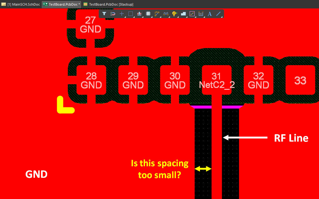
The example above is quite important as many application notes for components with RF outputs will recommend exactly this type of routing, possibly with a via fence along the trace. The intent here is to isolate the RF trace from EMI that may come from other portions of the layout, or from some external source. However, these same application notes will generally give an overly conservative guideline on the spacing between the RF trace and the nearby GND copper pour. So just how close can you place the ground pour to your controlled impedance trace?
Is it a Microstrip Transmission Line or a Coplanar Waveguide?
For the moment, I want to focus on single-ended microstrips because they are conceptually easy, but everything I’m about to write applies equally to striplines. The same ideas also apply to differential pair routing.
If the surface layer ground pour in the above image is too close to the trace, then we have a coplanar waveguide, not a microstrip. Theoretically, when the surface layer ground pour is an infinite distance from the trace, then we are back to a microstrip. If you bring the ground plane too close to the trace, you will alter the impedance of the microstrip due to the parasitic capacitance between the edge of the trace and the ground pour. This is why single-ended microstrip transmission lines and single-ended coplanar waveguides don’t always have the same trace width; the coplanar waveguide generally requires a smaller width to have the same impedance as a microstrip on the same stackup.
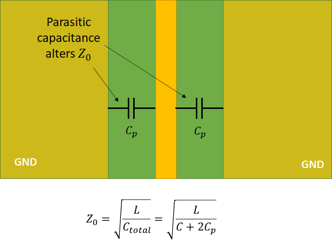
From the above, we can see why coplanar waveguide traces may need to be smaller than a microstrip on the same layer and stackup. The parasitic capacitance increases the total per-unit-length capacitance of the trace, so L needs to be increased to compensate, thus bringing the impedance back to 50 Ohms. In the next section I’ll use this idea to test when the ground pour is too close to the trace by looking at the impedance deviation from a 50 Ohm target as a function of ground clearance.
Testing the “3W” Rule
There is actually a rule of thumb here. This is the “3W” rule, which states the spacing between the trace and the nearby ground pour should be at least 3x the trace width. As we’ll see momentarily, this guideline is overly conservative and does not account for multiple factors. In reality, the minimum required spacing will depend on:
- The routing style (microstrip vs. stripline)
- Whether single-ended or differential pair routing is used
- The dielectric constant of the substrate
- The distance between the trace and its ground plane on the next layer
Since we’re looking at a situation where you need to determine the trace width required for controlled impedance, I’m going to test the 3W rule by comparing the trace width required to produce a 50 Ohm impedance microstrip with a coplanar waveguide of the same impedance. I’ll do this for various layer thicknesses so we can see how this parameter affects the required ground clearance. Here, the goal is to determine the minimum spacing needed to produce a coplanar waveguide with the same impedance and trace width as a microstrip.
Results
I first generated a set of curves showing the microstrip width, stripline width, and coplanar widths (interior and surface layers) required to produce 50 Ohm impedance on a 370HR Isola laminate (Dk ~ 4.1, ~0.02 loss tangent @ 1 GHz). These calculations were performed in Polar. The image below shows these results and allows trace widths for each type of trace to be compared for a specific trace-to-ground pour spacing of 5 mils.
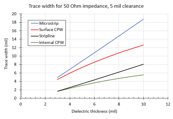
From here, we can see that there are specific stackups where a CPW and a microstrip/stripline will have 50 Ohm impedance and the same trace width, even though the ground clearance is quite close to the trace in the CPW.
The next graph investigates this further. It shows the minimum trace-to-ground spacing required to produce a 50 Ohm impedance microstrip and a 50 Ohm coplanar waveguide with the same trace width. Results are also shown for a stripline and a coplanar waveguide on an internal layer.
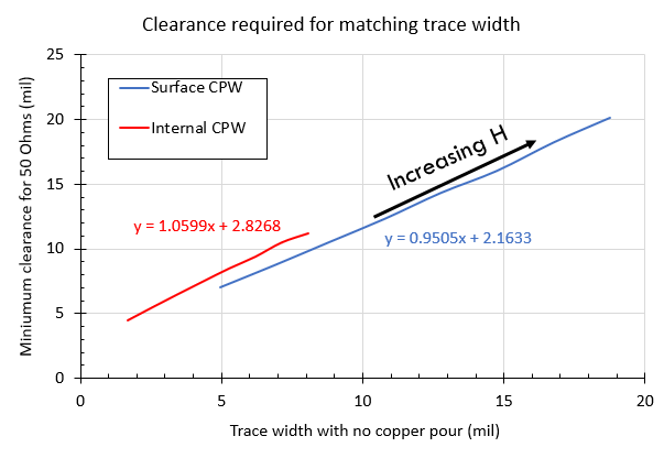
The interpretation of the above graph is very simple: this shows the minimum trace-to-ground spacing in a CPW required to produce the same impedance in a microstrip/stripline when they both have the same trace width. From here, we can finally generate our test of the 3W rule. Simply divide the y-axis data by the x-axis data to produce the following graph:
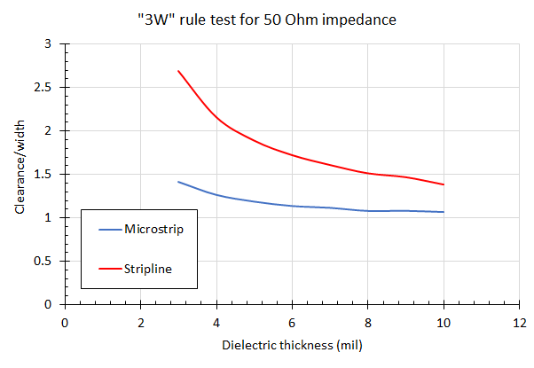
It’s quite clear that the 3W rule is overly conservative, except in cases with stripline routing in thin dielectrics. Follow it if you like as it will prevent excessive interference with your impedance. However, that distance might not provide the isolation you need. This is one area that can be tested with a field solver by looking at coupled network parameters and crosstalk coefficients between different interconnects.
Summary
From the above results, it should be very clear that the 3W rule used to determine ground-to-trace spacing between a microstrip and the nearby ground pour is overly conservative. Note that the above dielectric thicknesses are practical values you might find on a 4-layer or thicker stackup, depending on the laminate used for stackup construction. We can also see that, for a given distance to the ground plane, you can have much tighter clearance with a microstrip, whereas a stripline requires much larger clearance in thinner dielectrics. Eventually, when the dielectric gets thick enough, these two curves will converge on each other.
Determining an appropriate spacing for microstrip ground clearance starts with the best PCB stackup design tools. When you use Altium Designer®, you can easily determine the trace width and spacing required to ensure controlled impedance routing in boards that use grounded copper pour in your PCB layout.
When you’ve finished your design, and you want to release files to your manufacturer, the Altium 365™ platform makes it easy to collaborate and share your projects. We have only scratched the surface of what is possible to do with Altium Designer on Altium 365. You can check the product page for a more in-depth feature description or one of the On-Demand Webinars.
