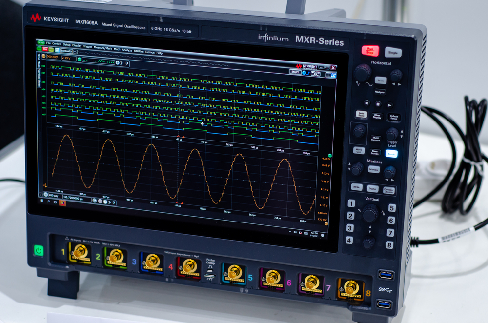
How to Use Input Impedance in Circuits and Transmission Lines
Input impedance is one of those terms that gets thrown around a bit without a lot of context. Designers who know the finer points of transmission line theory should understand how to use this to determine what qualifies as an “electrically long” interconnect, rather than just going with a 10% wavelength value as a rule of thumb. Input impedance follows a similar idea in circuits, although we don’t normally treat a circuit as having transmission lines connecting different components.
Input impedance is an important aspect of understanding transmission line connections between different components in electronics. Input impedance is primarily used in RF design, but it can be used to develop transfer functions in high speed design, which then can be used to predict impulse responses using causal models. One of the points that is almost never addressed in dealing with input impedance is how interconnects between components modify the impedance seen by propagating signals. I’ll show some simple examples of how this arises and how it determines the real input impedance seen by your signals.
Understanding Input Impedance
In an earlier article, I presented a set of definitions for transmission lines that includes the input impedance. Without repeating everything in that article, I’ll briefly summarize the important definitions as they relate to input impedance, characteristic impedance, transmission lines, and circuits.
Circuit Input Impedance
If we look at a typical circuit, it can have multiple impedances, as shown in the diagram below. In this conceptual example, we have a driver with some defined output impedance (Zout), and the circuit has various impedances that combine to form an input impedance. In the example below, the input impedance is just the equivalent impedance Zin = Z1 + (Z2||(Z3 + Z4)).
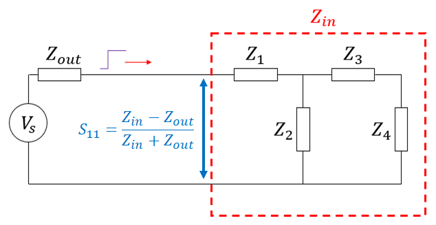
When the driver excites the circuit, there is a reflection coefficient (S11) between the driver’s output impedance Zout and the circuit’s input impedance Zin. By matching the impedances, we have either minimum reflection (equal input and output impedances) or maximum power transfer (conjugate matching), or both simultaneously for resistive impedances. What the input impedance doesn’t tell you is what happens between each of the elements inside the circuit. There could be reflections between any of the four impedances that make up the circuit.
Modern components that require impedance control will apply on-die termination, which will give a reliable impedance value over a broad bandwidth. At very high frequencies, the output impedance will become reactive again because of package parasitics (die capacitance and pin/bond wire inductance), which will limit power transfer from the driver to the load.
That covers the basics of a driver component that connects directly to a circuit. What happens when we now have a transmission line between the driver and the load circuit?
Transmission Line + Circuit
Now if there is a transmission line between the driver and receiver, we have a “new” input impedance located near the source component. This input impedance now depends on the transmission line characteristic impedance, the length of the line, and the propagation constant along the line.
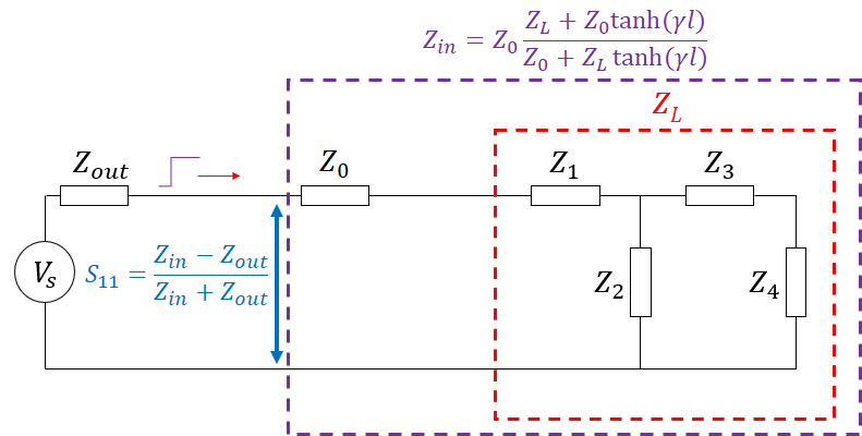
This is where we get a definition for a transmission line critical length; it’s based on the relationship between propagation constant, line length, and frequency, any rule regarding rise time is just an approximation and should not be used in high speed design or RF design. This is also one of those instances where most guidelines end and they do not continue to explore real situations in RF design or high speed design.
Input Impedance of Cascaded Elements
Now we need to consider a real situation where you have multiple elements on a transmission line, or even multiple lines, all cascaded to form a more complex network. What is the input impedance in this case?
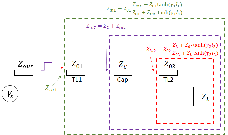
Let’s consider a common situation you might encounter in RF design, or in PCIe routing, where you have an AC coupling capacitor placed on the line. In an RF situation at radar frequencies, or with very high bandwidth signals found in newer PCIe generations or possibly high-gig Ethernet, the interconnect will act like there are two transmission line sections between each section of the line. What then is the input impedance with three elements cascaded?
The answer is: the input impedance seen at the source is related to the input impedance in all downstream sections. This is an inductive problem as defined in the diagram below. The capacitor will have its own input impedance value (ZinC), which depends on the input impedance of transmission line #2 and the load impedance. Both input impedances will determine the input impedance of transmission line #1.
Hopefully, you can see how this inductive reasoning continues indefinitely. The above situation is about as complex as you’ll get in a high speed digital system unless you have to traverse a connector, in which case you’ll deal with cascaded S-parameters. In RF systems it can get very complex if you now have to design impedance matching networks and the size of the system could get large as you work to match impedances between each section of the system. There is a great paper on the implementation of this method for branched and cascaded systems in JPIER:
One outstanding question that should arise from the above system: what are the S-parameters as seen at the input? Because we have a cascaded system, you would need to determine the cascaded S-parameter matrix for this network. Using the iterative input impedance shown above gives you S11 at the input port, but that’s it. To get the full S-parameters, you would need to use a matrix calculation involving a cascadable parameter set; ABCD parameters are ideal. In fact, if you calculate this using MATLAB, their documentation states that they use an ABCD to S-parameter conversion to get the cascaded S-parameters for the above network. It’s a good idea to do these calculations as they can form the basis for measurements to evaluate your interconnect design.
Once you’ve determined the input impedance you need and developed design rules, you can route your traces and ensure signal integrity with the routing tools in Altium Designer®. When you need to evaluate signal integrity and extract network parameters in your PCB layout, Altium Designer users can use the EDB Exporter extension to import their design into Ansys field solvers and perform a range of SI/PI simulations. When you’ve finished your design, and you want to release files to your manufacturer, the Altium 365™ platform makes it easy to collaborate and share your projects.
We have only scratched the surface of what’s possible with Altium Designer on Altium 365. Start your free trial of Altium Designer + Altium 365 today.
