What VNA Measurements Can Teach You About Your PCB Substrate
Vector network analyzers (VNAs) are the workhorses of RF signal integrity measurements and have traditionally been used by microwave engineers to design microwave components and antennas. Today’s digital designers working with ultra-fast signals need to think in terms of mmWave concepts and understand what VNA measurements mean, specifically S-parameter measurements and resonant measurements. You can thank ultra-fast edge rates and high bitstream rates for pushing signal bandwidths well into the GHz regime to the point where digital designers now need to be analog experts.
If you know how best to interpret VNA measurements from your interconnects, you can learn something about the material properties of your substrate without destructive testing. You can also determine whether your design needs to change in order to meet your signal integrity goals.
What Does a VNA Measure?
The theory of operation behind a VNA relies heavily on network analysis for waves propagating in electrical networks. A VNA is sometimes compared to a DC multimeter, except that the VNA measures electrical behavior for AC signals. This is not exactly correct, but it’s a step in the right direction. The “N” in VNA stands for “network,” meaning the VNA measures how a sourced signal interacts with an electrical network. A typical measurement setup with an N-port device under test (DUT) is shown below.
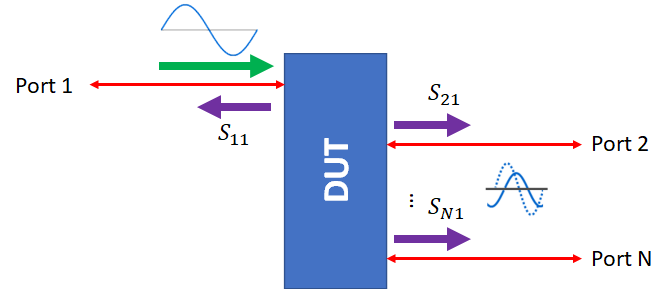
When a propagating signal is an incident on an electrical network, some power is reflected from the input port, and some power is transmitted through each output port. The reflected and transmitted power can be measured by the VNA (both magnitude and phase), which can then be used to determine the S-parameters for pairs of ports in the device. A VNA can also be used to measure voltage at the input and output ports, which then gives the voltage transfer function for the network. You can use these data in a range of other analyses.
By taking advantage of these characteristics of a VNA, material properties can be inferred from VNA measurements. In these measurements, you can use two classes of methods with the material to be examined placed as the DUT:
- Resonant methods: These involve using the VNA to compare the measured resonance frequency for a reference material and the material under test. This requires using a waveguide test structure with an established model for the resonance frequency as a function of Dk and geometry. S-parameters are not directly measured in this method.
- Non-resonant methods: Material characteristics are determined from S-parameter measurements (either reflected or transmitted power). Common reference structures used in this measurement are waveguides, transmission lines, open-circuit coaxial probes, or transmission through free-space.
VNA Measurements for PCB Materials
Here, I’d like to focus on a non-resonant S-parameter method as this is more common for designers who don’t work at laminate companies. There is one simple way to learn something about your material parameters and a more complex method to calculate dielectric constant/magnetic permeability directly.
Long Transmission Line Limit
One way to see how material properties affect signal behavior is to look at a long transmission line and its S21 measurements. In the limit of a long transmission line, you can quickly extract an average Dk value for the substrate material simply by looking at the slope of the S21 data on a log scale. You can then see how dispersion and the loss tangent affect insertion loss in the channel.
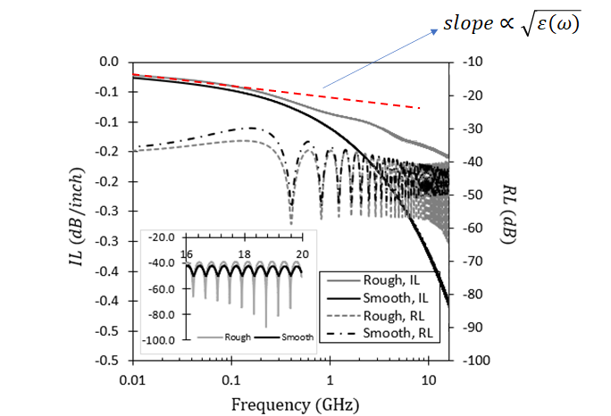
By comparing with a reference material, the dielectric constant can be determined by looking at the slope of the magnitude and phase of your S21 curve for your material under test. However, this is only valid when dispersion is relatively small, and the line is very long; obviously, this does not cover every situation, such as a reflection-dominated short transmission line. To get back to Dk values from measurements for any line length, we need more sophisticated conversion methods.
Non-resonant Transmission Line Methods
Non-resonant methods are more likely to be used as part of interconnect design and testing for high speed signals, where a real interconnect needs to be evaluated for use with a broadband signaling standard (e.g., USB 4). By looking at the non-resonant S-parameter data measurement with de-embedded fixtures, the data can be related back to material properties using standard models for your interconnect. This measurement process and conversion techniques for determining Dk/Df are valid up to the TEM limit for transmission lines and coplanar waveguides.
Suppose you have the S-parameters for your test channel after de-embedding. You can use one of the following methods to convert from your S-parameters back to a Dk, Df, and magnetic permeability values.
The table below lists some of the basic signal integrity requirements that apply in the PCIe 5.0 standard.
|
Method |
Inputs |
Outputs |
|
Nicholson-Ross-Weir method |
All S-parameters |
Dk, Df, magnetic permeability |
|
NIST iterative |
All S-parameters |
Dk, Df, magnetic permeability |
|
New non-iterative |
All S-parameters |
Dk, Df, magnetic permeability |
|
Short circuit line |
S11 only |
Dk., Df |
Going over the finer points of each method would take considerable space, so I’ll leave some of these as topics for future articles. In short, these methods rely on solving a transcendental equation for the complex dielectric constant of the PCB substrate material. The S-parameters are rewritten in terms of the channel’s input impedance, length, and propagation constant. The iterative methods listed above are then used to solve this equation at each frequency, starting from the S-parameter data. Take a look at this guide from Rhode and Schwartz for a complete process for these conversions.
Accounting for copper roughness makes the equation to be solved more complicated, but the solution algorithms for these problems are still rather simple. This is the topic of an upcoming paper I’m working on, and I’ll be sure to show how this can be used with VNA measurements in a later article.
Once you’ve gathered and analyzed your VNA measurements of your interconnects, it’s time to implement needed design changes so that you meet important design requirements. When you need to account for dispersion/loss/roughness in your PCB substrate, use the complete set of stackup design and layout tools in Altium Designer®. When you’ve finished your design, and you want to share your project, the Altium 365™ platform makes it easy to collaborate with other designers.
We have only scratched the surface of what is possible to do with Altium Designer on Altium 365. You can check the product page for a more in-depth feature description or one of the On-Demand Webinars.
