Transmission Line Impedance: The Six Important Values

When looking through the various transmission line impedance values, characteristic impedance and differential impedance generally stand out as the two important values as these are typically specified in signaling standards. However, there are really six transmission line impedance values that are important in PCB design. Sometimes there are seven, depending on which textbooks or technical articles you read.
Characteristic impedance equations can be found easily in a number of articles and textbooks, but the other common transmission line impedance values are more difficult to calculate. The reason for this difficulty is that it relies on the arrangement of multiple transmission lines and the strength of coupling between them. The other typical impedance value is the input impedance, which depends on the length of the line and any impedance mismatch.
Transmission Line Impedance Values
Here are the important transmission line impedance values to understand as part of PCB design and routing.
Characteristic Impedance
If you Google the term “transmission line impedance”, the definition of characteristic impedance is the most likely result you’ll see on the first page of the search results. Most designers are likely familiar with characteristic impedance as it is defined within a lumped circuit model. This model returns the following popular formula for characteristic impedance:
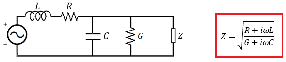
At sufficiently high frequency or with sufficiently low losses, the characteristic impedance becomes purely resistive and converges on the following value:

Characteristic impedance of a transmission line in the high frequency limit.
Note that the skin effect has been ignored here, which is applicable up to ~1 GHz bandwidth for digital signals. You can derive the values of L and C from the propagation delay and characteristic impedance by using standard formulas for different trace geometries. You can then use these circuit values to optimize your trace width and inductance and minimize transient ringing.
The characteristic impedance is sometimes called “surge impedance” and is related to the term “surge impedance loading.” This term is often used by power system engineers to quantify power transferred across a transmission line and seen at a load.
Even Mode and Odd Mode Impedance
Two transmission lines that are sufficiently close to each other experience capacitive and inductive coupling. This coupling is normally what determines crosstalk, but it also modifies the impedance seen by the signals on each line. When coupled lines are driven in the common mode (same magnitude, same polarity), the even mode impedance is the impedance seen by a signal travelling on one transmission line in the pair. A similar definition applies when the lines are driven in differential mode (same magnitude, same polarity):
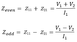
Note that the even and odd mode transmission line impedance values are defined in terms of Z parameters for a pair of coupled transmission lines:
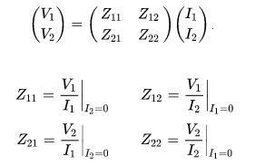
The Z matrix (also called impedance parameters) can be easily converted to S-parameters. It can also be generalized to multiple coupled transmission lines with common mode or differential driving. Take a look at this PDF for the equations required to convert Z-parameters or a characteristic impedance value to S-parameters.
Common Mode and Differential Impedance
Common and differential mode impedance values are related to the even and odd mode impedance values. Differential impedance values are normally specified for impedance matching of differential pairs, rather than odd mode impedance. The differential pair impedance depends on the characteristic impedance and the spacing between each end of the differential pair. The same applies to common mode impedance, except that common mode impedance arises under common mode driving.
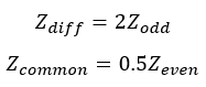
Physically, differential impedance is the impedance measured between two coupled transmission lines when the pair is driven in differential mode. Similarly, the common mode impedance is the impedance measured between two coupled transmission lines when the pair is driven in common mode.
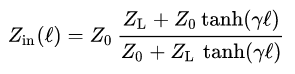
Input Impedance
This transmission line impedance value is important in impedance matching and can be used to quantify when a transmission line has surpassed the critical length; take a look at the linked article to see how you can quantify permissible impedance mismatch. Without repeating everything in that article, the input impedance depends on the characteristic impedance, propagation constant, load impedance, and length of the transmission line:
Integrated Transmission Line Impedance Calculators
Several equations are presented here, and these equations describe ideal situations that do not account for the complex geometry of a real PCB. However, they are still a good place to start when designing transmission lines. Circuit models can be used to approximate coupling between lines in terms of mutual capacitance and inductance, which can then be used to determine even/odd and common/differential impedance values.
When you need extremely accurate transmission line impedance calculations, you need to use a route that has an integrated electromagnetic field solver. This gives you very accurate impedance results with real PCBs, as well as signal behavior on the rising and falling edges. This nicely accounts for complex parasitics that cannot be brought into circuit models, and it allows a designer to account for length tuning geometries along the lengths of coupled transmission lines.
The layer stack manager and routing tools in Altium Designer® include an electromagnetic field solver that creates an accurate impedance profile for common trace geometries. This makes controlled impedance routing quick and easy, and it gives you sub-mil accuracy when designing transmission lines. Now you can download a free trial of Altium Designer and learn more about the industry’s best layout, simulation, and production planning tools. Talk to an Altium expert today to learn more.
