How to Combat Power Supply EMI in Your PCB
Power supplies are one of those systems we all tend to take for granted. Everyone’s first task in power supply design is usually to ensure the voltage and current output reach the desired level, probably followed by thermal considerations. However, due to safety issues, EMC requirements, the use of higher PWM frequencies, and the need for smaller packaging, power supply EMI should be a major design consideration. Power supply EMI should be ignored at a designer’s own risk as failing to pass EMC testing will lead to a bevy of redesigns that waste time and money.
With that being said, what are the major sources of power supply EMI, and how can power supply designers keep them in check? EMI from a power supply primarily manifests itself as conducted EMI being driven to a load, but there is also radiated EMI from the device, particularly when designing high-current switching regulators. While we can’t cover every single source in this article, I’ll compile a list of strategies that can help you get started solving some common power supply EMI problems.
Find the Cause of Power Supply EMI
As I mentioned above, power supplies primarily output conducted EMI, although there can be particularly strong radiated EMI in switching power supplies. When we think about EMI in power supplies, we need to consider the topology, and whether we want to address unwanted currents or unwanted emissions, when planning the PCB layout. A simple linear regulator or an LDO will have fewer problems to address than a high-frequency, high-current switching regulator.
In the table below, I’ve outlined the three common sources of EMI and their causes in power supply units and in on-board regulator circuits. Just for a moment, we sometimes need to distinguish between EMI that happens inside the power supply and EMI that is received by the board connected to the power supply. In reality, the magnitude of EMI in each type of system is a matter of scale; the fundamental mechanisms that produce EMI are the same in embedded power regulators and power supply units.
|
|
|
|
|
|
|
|
|
|
|
|
Volumes have been written about each of these areas, and each area can’t be taken in isolation. For example, various operation modes (e.g., ringing) and switching parameters (high PWM frequency) can combine to produce common-mode currents, which then generate some EMI or are conducted to downstream components to reduce total power delivery.
Let’s look briefly at each of these areas to see how they relate to power supply EMI.
Common-mode Currents
The drivers of common-mode currents are a bit counterintuitive. Common-mode currents are an electrical effect, meaning driven by changes in the electric field, so common-mode currents in power supplies are mediated by parasitic capacitance back to the chassis, rather than parasitic inductance. The graphic below shows an example of input current in a DC regulation section of a power supply appearing as common-mode noise on the PWR/GND rails.
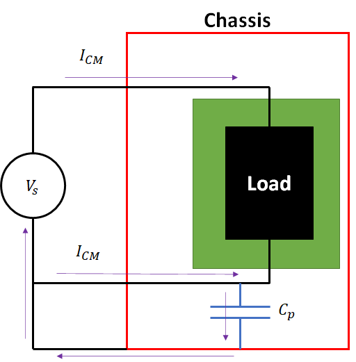
Note that this current path can appear in the system even after input common-mode noise is filtered from the AC mains input. It can also have a very large loop inductance, creating a new location to emit or receive EMI.
Why should this occur to begin with? The reason is that there is a potential difference between Point A in the above diagram and the chassis, allowing some current to conduct back to the mains via parasitic capacitance. A similar problem can happen in Ethernet boards with split ground sections, where the common-mode noise can couple to the PHY side of an Ethernet net link.
The solution: It depends on how common-mode currents are entering the system. For conducted currents from AC mains, you’ll want some filtration on the output of the power supply. A common-mode choke is standard, or you can use a common-mode current filter with low-pass topology. A pi filter can be used for extra filtration of differential-mode noise. In some systems, like industrial Ethernet switches, common-mode currents will happen, but your job is to prevent them from conducting into sensitive circuitry by tracking your return paths.
What Causes Parasitic Ringing?
In the above table, I've identified a few causes of ringing that can occur, particularly in discontinuous mode operation. However, parasitics can also cause the conditions for damping in the design to be modified, leading to an underdamped resonance with ringing. There are many parasitics found in real components that will influence ringing. Ringing is not exactly a form of EMI as it is caused by reactive elements in real circuits. However, ringing in its various forms can contribute to other forms of EMI (see this article for an example), so it should be included in a discussion of EMI, especially in power supplies. Some parasitics that are prominent participants in ringing include:
- MOSFET lead-wire inductance, body capacitance
- Inductor/transformer winding capacitance
- Parasitic inductance in current paths in the PCB layout
- Interaction between parasitics and intended RLC elements in the circuit
The parasitics and desired components in the power supply layout form an equivalent RLC circuit, which could exhibit an underdamped resonance. Ringing appears as differential-mode noise on the output with power spectrum spanning into high MHz frequencies, depending on the resonant frequency of the equivalent RLC circuit formed by parasitics.
The solution: Use components with smaller parasitics, which may mean physically larger or smaller components. Unfortunately, this is not as easy as it sounds, both in practice and in simulation. In addition, you need to focus on the parasitics that matter most in your design, and you’ll need to accept that your layout will never be totally free of parasitics.
Radiated EMI
Radiated EMI has two principal sources. First, it occurs in bursts in a switching regulator whenever the MOSFET switches, which also generates some conducted EMI that spans over a broad power spectrum (see below). Second, common-mode currents are also sources of radiated EMI. The radiation pattern from these two sources can be very complex and can span over multiple harmonics.
The solution: You need to use low-pass filtering to try and remove some of the conducted (differential mode) EMI from the power supply output. Radiated EMI is reduced significantly by focusing on reducing common-mode currents, whose radiation can be ~100x as strong as differential-mode radiated EMI (see the example measurements below). Radiated EMI from switching is largely unavoidable, although it can be suppressed with ground pour near the switching section and ensuring low loop inductance routing.
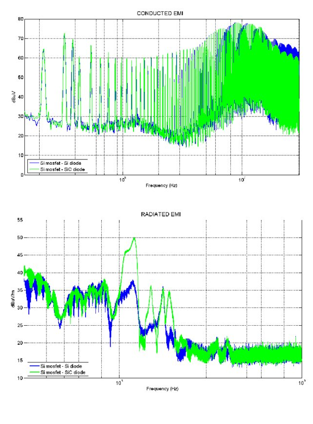
Note that the conducted EMI spectrum shown above could also appear in the radiated EMI spectrum. This can also be seen from switching crystals, which can radiate strongly due to large loop inductances along the path of the clock signal line. The same can occur when a high frequency PWM signal is not routed near a large reference plane. This secondary problem is related to routing, rather than simply the nature of switching in MOSFETs or other switching components.
In the event that these measures don't do the job, there are shielding measures that can be implemented on the board. Most designers are probably familiar with shielding cans, which are mountable to the board and can be used to target specific circuits or groups of components. Then there are enclosure solutions, such as conductive tapes, conductive gaskets, mesh shielding materials, and the like that can be mounted to the enclosure. Be mindful of how you ground out these solutions; the proper usage required to create a Faraday cage in the design depends on how you've defined "ground" in your system (i.e., earth, chassis, or system ground).
Diagnosing EMI Problems in Power Supplies
SPICE simulations are great for examining the topology and electrical performance of your power supply circuits, particularly switching regulators that may produce conducted noise or radiated noise. However, these types of EMI can’t be fully diagnosed with simple SPICE simulations because they can depend so heavily on the physical layout. A field solver utility can help you identify locations in the layout with strong radiated emission, strong ringing, and common-mode currents. Doing this properly requires importing your design directly into a field solver utility so that the tool can consider your layout directly.
When you need to investigate power supply EMI and change your design to reduce EMI, you can use the complete set of PCB design tools in Altium Designer®. For more advanced calculations involving conducted or radiated EMI, Altium Designer users can use the EDB Exporter extension to import designs into Ansys field solvers. This pair of field solver and design applications helps you verify your layout before you begin a prototyping run.
When you’ve finished your design, and you want to release files to your manufacturer, the Altium 365™ platform makes it easy to collaborate and share your projects. We have only scratched the surface of what is possible to do with Altium Designer on Altium 365. You can check the product page for a more in-depth feature description or one of the On-Demand Webinars.
