EMI Case History — Noise Problems And Their Solutions — Part 1

There is an old saying about experience being the best teacher but, more often, the appropriate adage is: “Experience is a hard teacher because she gives us the test first, the lesson afterward.” (Vernon Law). This can definitely apply to the PCB product development process when problems missed during design can arise when the working hardware is put into operation.
The foregoing is an apt description of an EMI design issue that we encountered during a consulting project. Our services focused on helping to determine how best to fix that EMI noise problem. The nature of the problem, the different fixes tried to correct it and the final solution is the focus of this article. Part 1 of this article will describe the origin of the problems that created the EMI noise issue while Part 2 will describe the various solutions researched and the final fix that was created.
Note: A far more detailed explanation of this case history is provided in "How Ground Bounce Can Ruin Your Day" a paper that was authored by Sunumani Krishnan and Benjamin Dannan, and presented at the DesignCon technical conference in January 2020. The complete paper is provided in the proceedings of that conference.
The Machine and The Problem
The machine in question was the next-generation autonomous cleaning robot used for cleaning the floors of big facilities, such as warehouses. That robot contains a touch-screen LCD display.
During the EMC pre-compliance test effort, it was determined that there were multiple EMI noise issues coming from the system. Further troubleshooting of these issues narrowed the problem down to the aforementioned LCD displays.
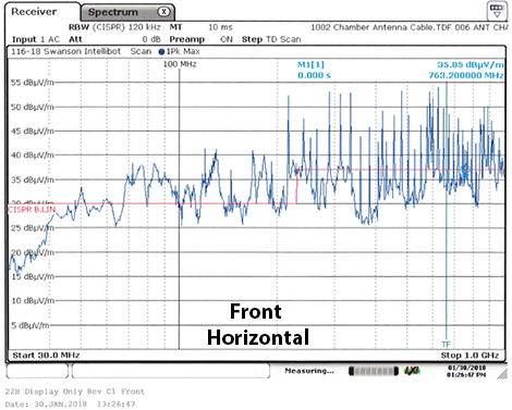
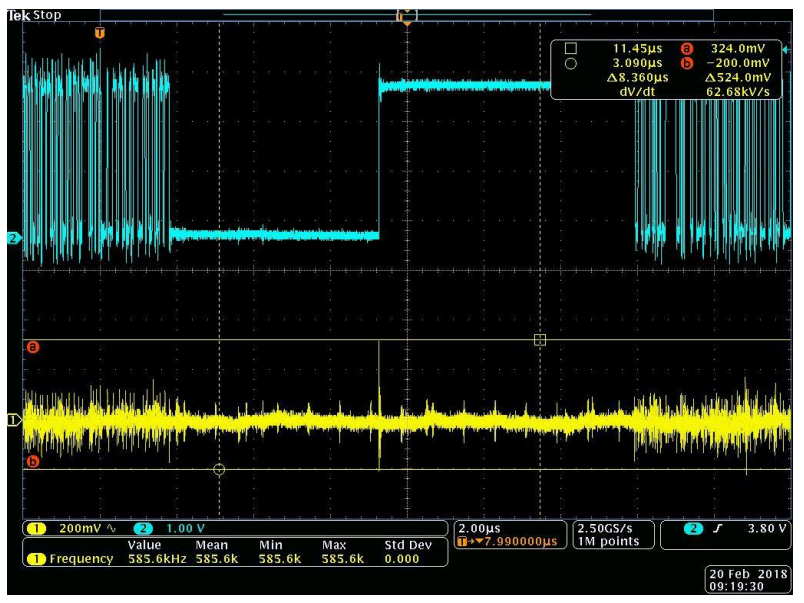
The entire system was tested in an EMC chamber with a far field antenna, which was kept at a three-meter distance from the system. In this instance, the noise shown in Figure 1 is from an EMI noise scan of the entire robotic system with the LCD installed.
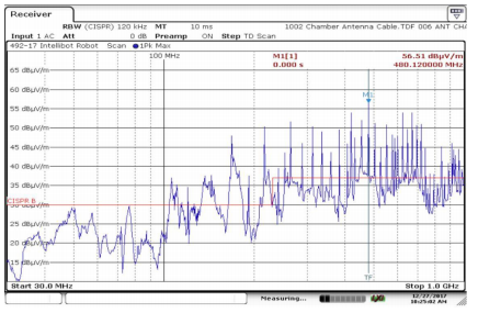
The LCD display used in the robotic system was then tested separately and powered with an external power supply in a three-meter EMC chamber with a far field antenna. The EMI measurement of the LCD display when powered by a 24V external power supply is shown in Figure 2. It was verified that the 24V power supply had no EMI noise prior to connecting it to the LCD display for additional EMI noise measurements. As shown in Figure 2, there was a significant amount of EMI in the system from ~200 MHz to 1 GHz, which was later verified to be created by the ground and supply bounce from the LCD display. It was then discovered that when this LCD unit was connected to a system with multiple printed circuit board assemblies, the noise generated from the LCD conducted onto various cables which then radiated throughout the entire system.
The LCD display assembly in question was composed of an LCD display unit and a driver printed circuit board assembly (PCBA). The LCD driver PCBA used a STM32F429IIT microcontroller with a 176 pin LQFP package. The driver PCBA used a 24-bit RGB (red green blue) bus to interface to the LCD display. Further investigation also revealed that the LCD driver PCBA provided only a few return paths on the microcontroller using this RGB data bus. The LCD driver PCB stackup analysis showed traces routed in the power and ground layers of the PCB that was compromising their integrity as planes. In order to find a correlation between the EMI and the source of the issue on the LCD display, further investigation was done on the power and ground rails of the LCD display assembly.
The Root of the EMI Noise Problem
It was determined that ground bounce was the culprit behind the LCD display problem. As noted in earlier articles (as well as the Reference 1 book listed at the end of this article), the current transients required to charge up and discharge logic lines as they change state are the primary sources of ripple on Vdd and the source of Vcc and ground bounce in the IC package leads.
Delving a bit more into what transpires, when logic lines switch from logic 0 to logic 1, the current that is supplied by the power system must pass through the inductance of the Vcc leads of the IC package. When the logic lines switch from logic 1 to logic 0, the parasitic capacitance of the transmission lines must be discharged through the inductance of the ground leads of the IC page. This results in two different types of noise. In switching from 0 to 1, the current required to charge up the transmission line must be drawn from the capacitance of the power subsystem. If this capacitance is not large enough and capable of responding at the speed of the switching edges, the result will be ripple on Vcc. In addition, the power leads of IC packages always contain unwanted inductance. Current transients flowing from this inductance produce Vcc and ground bounce.
These EMI noise transients limit the practical width that can be used for single-ended data buses and they are a major source of logic failure in product designs. What was occurring in this instance was ringing on both the supply (power) and ground rails.
Finding a Solution
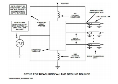
Using the test setup from Speeding Edge shown in Figure 3, the supply and ground bounce created by the LCD unit was tested.
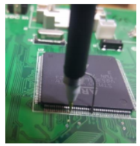
The testing began with the Rev A version of the LCD PCBA. The measurements shown in Figures 5 through 7 were captured with a Tektronix MDO4054C oscilloscope connected to a low inductance probe. The probe is shown in Figure 4.
As shown in Figure 5, ringing was found on the supply (3.3V) rail and output line. The peak-to-peak value of the ringing on the 3.3V supply rail was 524 mV.
As shown in Figure 6, ringing was also discovered on the ground rail and output line. The peak-to-peak value of ringing on the ground rail was 748 mV.
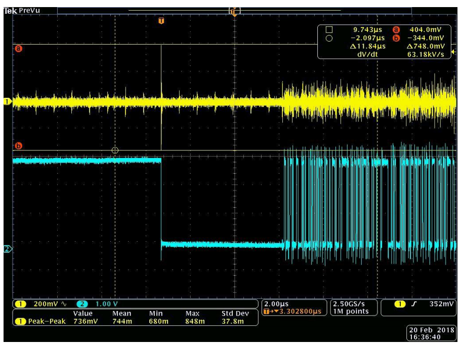
It was later realized that this ringing was being coupled to all the data lines as shown below in Figure 7.
It was not possible to use decoupling capacitors to contain this EMI noise. The amount of EMI noise generated by these transient currents was too large. In fact, if decoupling capacitors were added it would turn the system into a parallel resonant circuit. The ringing would actually become worse because of the oscillations that would be created during edge transitions.
The impact of the significant EMI noise issues created by the supply and ground bounce from the improperly designed LCD driver PCB forced an investigation for a proper solution to mitigate these issues.
NEXT: PART 2, TESTING VARIOUS OPTIONS ON THE PATH TO A SOLUTION
Have more questions? Call an expert at Altium or continue your study of adopting signal integrity in your high-speed design process.
References:
- Ritchey, Lee W. and Zasio, John J., “Right The First Time, A Practical Handbook on HighSpeed PCB and System Design, Volume 1.”
- Krishnan, Sunumani and Dannan, Benjamin, “How Ground Bounce Can Ruin Your Day,” Presented at DesignCon 2020.