DIY Vapour Phase Reflow Control Shield
With all the projects I’ve been working on, I want a better way to do reflow soldering during board assembly than just using a hot air rework station. Initially, I was looking at converting a toaster oven to run picoReflow, and building a Pi Hat for the required electronics but I was finding that a good convection toaster oven on Amazon was starting to look rather expensive for the quality of work it would do. Another factor that I had to consider was the size of the oven as I’m working on a high power LED panel project, and a couple of other LED panels which will be on metal core boards. The high power LED panels did not look like they would fit into the toaster ovens I was looking at, or if they did that there would be enough heat to prevent defects.
Some of my first commercially manufactured boards were made by a small assembler who only had a vapor phase reflow oven rather than the large multizone convection ovens you see in most assembly lines. They were mostly working on specialized aerospace/military and mining boards that had strict requirements that the assembler told me were easier to meet with the vapor phase reflow process - this gave me my initial spark of interest into vapor phase reflow soldering. Fast forward to a few years ago, and there was a discussion on the OpenPNP group about reflow soldering methods where someone had a relatively low cost vapor phase reflow oven, which again got me interested in vapor phase soldering. Most vapor phase reflow ovens cost almost as much as a multi-zone conveyor oven that can handle orders of magnitude more boards per hour, but the ones from Imdes are far cheaper.
Late last year, when I was trying to buy a toaster oven to convert to a reflow oven, I started looking at what would be involved in making my own vapor phase reflow oven. It turned out for small batch production, there really isn’t much to the machines mechanically or electrically, so I could potentially build a machine for very high quality reflow soldering in my office without much effort or expense. The Galden liquid is relatively expensive, but the quality and repeatability of vapor phase are worth the price.
Running My Vapor Phase Reflow Oven
In this article, I’m going to build an Arduino-style shield for running the vapor phase reflow oven I’m working on. Rather than using an Arduino, I’m going to be using the board with the STM32F746 Discovery kit that includes a 4.3” TFT touch screen. With the powerful processor, it is relatively easy to develop a user interface using the TouchGFX library, which is now free. Originally, I wanted to build the entire board myself using the STM32F746 or the cheaper STM32F750, but the engineering effort required for a one-off build isn’t worth it, and with an 8 layer board, the discovery kit costs less than the price of manufacturing a single board, even at low-cost PCB suppliers!
I won’t be covering the machine build or testing in this article, if you’re interested in seeing an article or video on the machine build, programming and use, please leave a comment!
As always with my projects, you can find the design files available under the extremely permissive MIT license over on GitHub. You can use the project files to build your own board, base a product on it, or even see the design as is if you want. If you’re looking for the components used in this project for your own design, you can find them in my Celestial Library, an open source Altium Designer® Library.
Above is the PCB design you'll be reading about in the Altium 365 Viewer; a free way to connect with your co-workers, clients, and friends with the ability to view the design or download with the single click of a button! Upload your design in a matter of seconds and have an interactive way to take an in-depth look without any bulky software or computer power.
What is Vapor Phase Reflow?
Vapor phase reflow, or condensation reflow soldering, uses a liquid that has a high boiling temperature. Water boils at 100 °C at sea level and turns into vapor (steam). Vapor phase reflow soldering works on the same idea, but Galden boils at a range of temperatures that are useful for soldering. Galden is a completely inert liquid, and as long as you keep it below its decomposition temperature, it is safe to use. You don’t want to breathe the vapor from it, but it is safe to handle and will not react with anything on your circuit board.
I plan to use Galden LS-230, which changes state at 230 °C. This means that if I heat the liquid over 230 °C, it will turn to steam that will condense on the circuit board and every other component on the board. Colder sections of the board will have more condensation, which in turn means more heat transfer to those areas of the board. This means that if you have a board with a giant transformer/inductor or other large heat mass right next to an 0402 component, your board will still reflow well as everything comes up to temperature fairly evenly. With the wide variety of projects I have been working on and are still on my todo list, this is a fantastic asset.
Galden is also almost twice the mass of water for a given volume, making it great for soldering. Because the liquid and its vapor are so heavy, it creates a vapor layer over the board, which displaces any air. This means that the reflow soldering happens in an essentially inert atmosphere. As the boards are reflowed in an inert atmosphere, the solder will experience very little oxidation as it melts, which gives you fantastic quality solder joints free of oxides.
Finally, because Galden LS-230 boils off at 230 °C, it’s not possible to heat the board beyond this temperature. Your board will have perfectly even heating with no hot spots. There is also no radiant heat from ceramic or IR elements that could cause some components to have very high temperatures while the board is still cold in other areas. For me, this means it's a really easy process to tune, with no worries about melting surface mount connectors or finding your surface mount switch is a puddle of plastic, despite the solder not having quite melted yet. It also means that on large boards with a lot of thermal mass, like the LED panels I’m working on, you won’t see some components reflowed and others where the solder hasn’t even melted at the end of the cycle.
There are a couple of major downsides to vapor phase reflow soldering: cost and cycle time. As you heat up the air within the reflow chamber, it expands and needs to escape, some Galden will go with it, and you may have some Galden trapped somewhere on your board when you remove it leading to losses of the reflow fluid. Galden is not cheap, with the Imdes ovens I mentioned earlier losing a dollar or two of fluid each cycle. For me, this is an acceptable rate of loss as I’m not using it for production work. If you were to perfectly seal the chamber, you would have to take this into account during the design phase, as you will create a pressurised vessel that needs to be able to cope with the pressure differential without exploding.
With an infrared or convection oven, there is very little thermal mass to cool down, as you can simply flush the hot air out of the oven. With the cost of Galden, this is the last thing you want to do, which leaves you with a lot of thermal mass in the system. Your ramp times may be longer in both heating and cooling compared to convection or infrared ovens, which increases cycle time. To combat this, my oven design uses a 1.1kW heater and over 200W of cooling fans.
In short, despite having a cost per cycle beyond simple power usage, vapor phase reflow makes home or office DIY reflow solder oven incredibly reliable, consistent and high quality compared to what you can achieve with similar priced DIY or commercial systems.
Schematic Design
On with the project itself then! As I mentioned earlier, there isn’t much to a control system for the oven. The entire system is essentially just several thermocouples, an output for a solid state relay and a fan controller. Because this is a shield for a complex microcontroller board, I don’t need to worry about DDR routing, high speed flash or LCD control lines which really simplifies things.
Thermocouple Cold Junction Compensation
I’m going to have three thermocouples in the oven:
- One directly attached to the heating element to ensure it never exceeds 300 °C, the decomposition temperature of the Galden,
- One attached to the side wall of the oven, to probe the air/vapor temperature,
- One attached to the board platform as another temperature reference in the oven.
The first thermocouple is purely for safety—if I ran my PID temperature controller on the vapor temperature alone, it is possible the heating element could cause the pan above it to reach the decomposition temperature of the Galden. This high temperature could create toxic fumes, and I’m not too keen on toxic fumes. The other two thermocouples are for process monitoring and control to ensure the lower chamber has filled with hot fluid and reflow has completed before starting the cool down cycle.
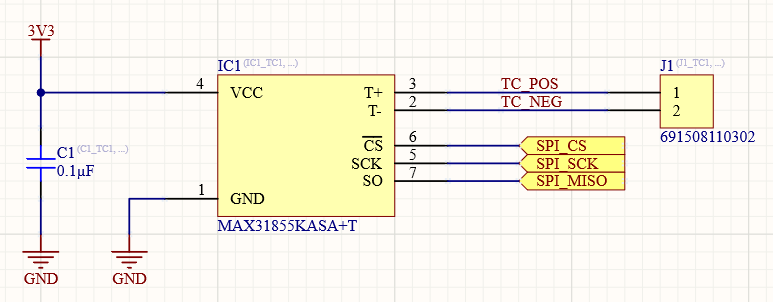
Each thermocouple is a single channel with a MAX31855 thermocouple to digital converter. This thermocouple controller applies cold junction compensation. I’m using the K variant in my design which is slightly more expensive but has higher accuracy than the other variants. Each thermocouple has a wire-to-board terminal block for connecting the thermocouple to the shield. Thermocouple cables must be crimped or otherwise mechanically connected to the board, as solder will not adhere to the wire. I could have used a thermocouple specific connector here, however, the thermocouples I purchased for the project do not have these connectors on them, making a simple terminal block easiest.
In my previous current monitor and controller project, I talked about using the Repeat command on a top level schematic to create multi-channel designs. I mentioned that typically the only time I might not use the REPEAT command on the ports within the sheet symbol, was for connecting a communications port. At the time of writing, I had no idea that it would be so soon after I would have a project to demonstrate that!
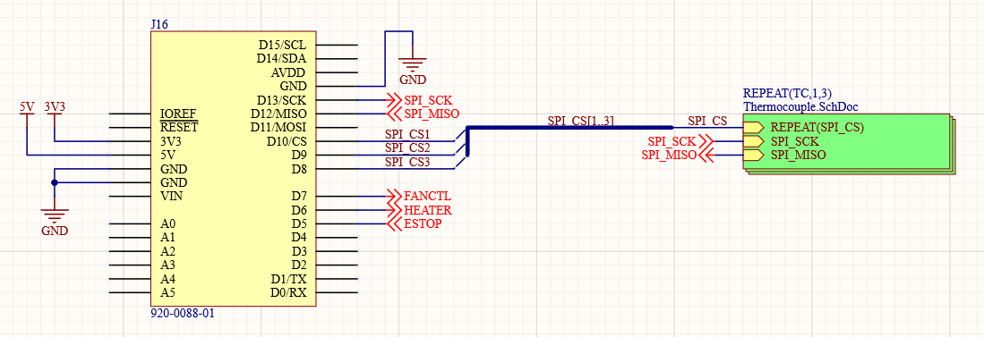
For each thermocouple channel, we want the master in/slave out and clock channels going to the microcontroller in parallel, so we don’t use the REPEAT command on those ports. The chip select channel however we want to have per channel, so I am using the REPEAT command for the SPI_CS port. The MAX31855 does not have a master out/slave in pin, so does not need a SPI_MOSI connection.
Heater
The heater will be controlled by an off-board solid state relay. This allows me to switch the AC heater easily without running mains AC on my board, which I try to avoid whenever possible.
The solid state relays I’m using have a 4-32V input which requires about 20mA. This is both higher voltage and higher current than the STM32F746 can provide, so I’m using a low cost n-channel MOSFET for the output.
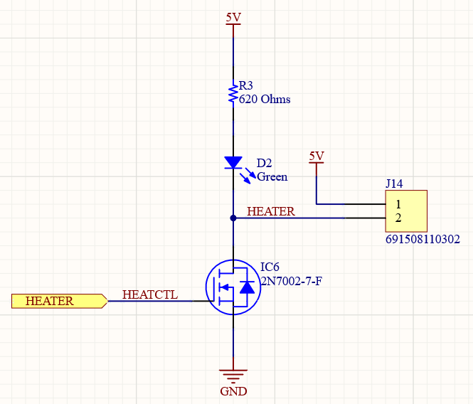
I also have an LED on board to indicate that the heater is on. Again, I’m using a simple wire-to-board terminal block for the connection.
Emergency Stop/Safety
I want to have an emergency stop button on the machine that does not go through the microcontroller. This will shut down the heater and turn on the cooling fans, rather than just cutting power to the machine as a whole. If the microcontroller stops responding for some reason, I want a way to shut off the heater and cool the process chamber down to a safe temperature as quickly as possible.
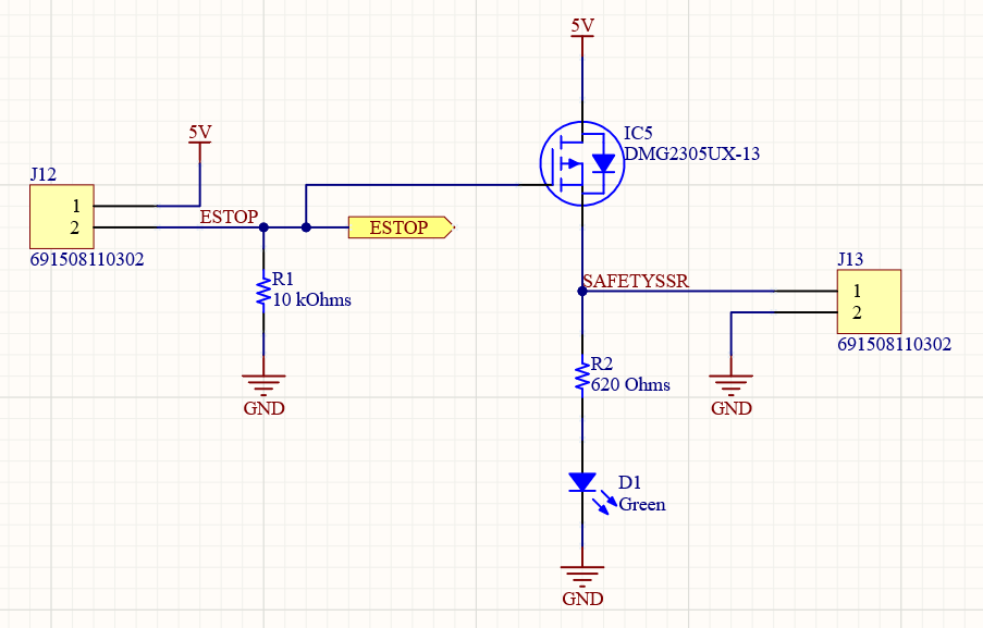
I have another terminal block which the estop button will short when it is pressed. This has a P-Channel MOSFET going to yet another terminal block which will control a second solid state relay. The heater’s live/hot wire will be wired from mains, through both solid state relays in series, and then to the heater. Both solid state relays need to be on for the heater to run. With a low level signal on the MOSFET, the safety solid state relay will be active.
Fan Controller
The fan controller is the most complicated part of the entire project, but is still a very simple schematic. To allow either the microcontroller or the estop to turn on the fans, I have an OR gate with both the estop and microcontroller inputs connected to it. If either input is high level, it will signal the FET driver to turn on. I’m using a Microchip MCP1402T MOSFET driver to drive the gate of a beefy MOSFET. The OR gate itself could turn the MOSFET on, but not with sufficient voltage to reach the minimum RDS-ON of the MOSFET. The MOSFET has an incredibly low 1.6mOhm minimum RDS-ON which is going to keep it running cool under load, but it needs more than 5V on the gate to reach that. A gate driver for this application is perhaps overkill, but it does give me options for PWM control and such in the future, if I want to add that capability.
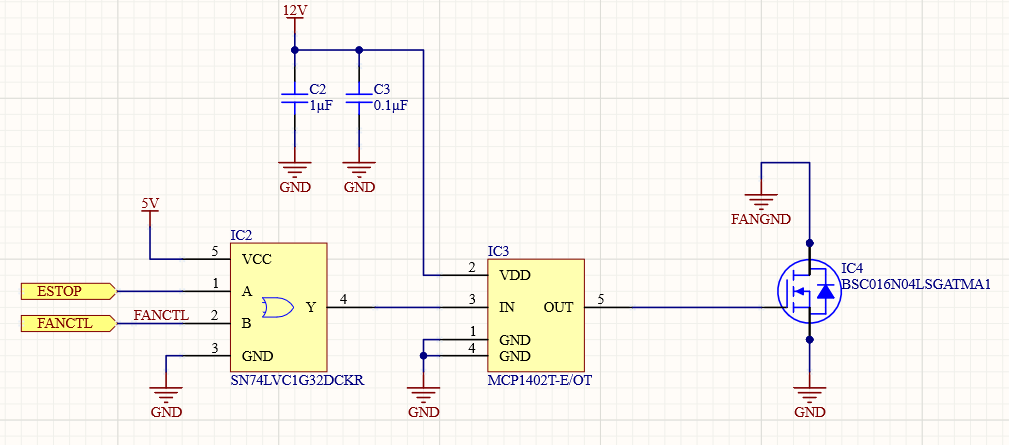
I’m using 8 Mechatronics MR9238E12B-FSR fans, which are 12V fans rated for 2.3A. When searching for fans for this project, I downloaded the Digi-Key results for the size and airflow I wanted and calculated the highest airflow per fan opening area per dollar, basically giving me the highest volume of air for the lowest price. I want a lot of air, not only to rapidly remove heat from the process chamber but also to ensure that the exhaust temperature of the air is as cool as possible. By having a very high volume of air, the hot air will hopefully be well mixed with cool air so the exhaust will not melt things around the machine.
With 8 of these fans on the machine, I have 18.4A of current draw going through the MOSFET so I’m using a large barrier block rated for 20A per pin to supply 12V to the board. For wiring convenience, have a terminal block per fan.
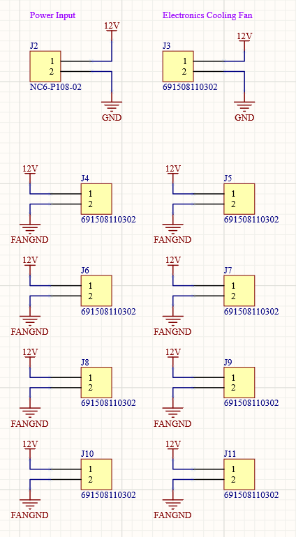
I also have an additional 12V ‘always on’ terminal block for a small cooling fan to provide a continuous flow of air through the electronics compartment. I don’t anticipate much heat transfer to the electronics compartment with the amount of insulation I’m using, but a simple fan will ensure that hot air can’t build up and overheat things.
Input Power
Rather than building a 12V to 5V regulator on the shield, I’m simply using a second low cost AC-DC switched mode power supply for providing 5V to the electronics. The 12V/250W power supply will be under a lot of load when the fans come on, so I wanted a stable, dedicated power supply for the electronics to run on, keeping the 12V supply for just the fans.
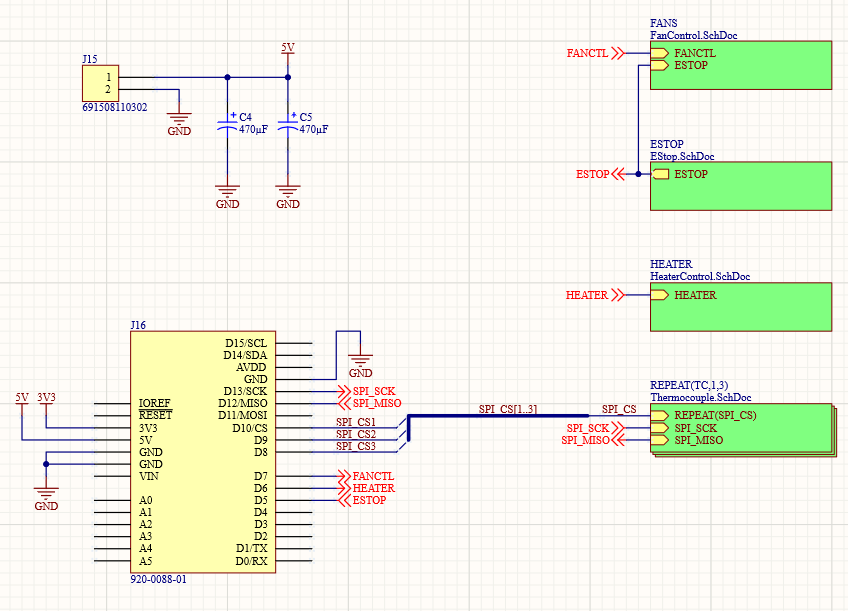
My top level schematic has the terminal block for the input power, as well as a couple of large, cheap capacitors to smooth out the supply. The 3.3V regulation is provided by the STM32F746 Discovery board and I’m not putting enough load on it to require a dedicated regulator for the shield.
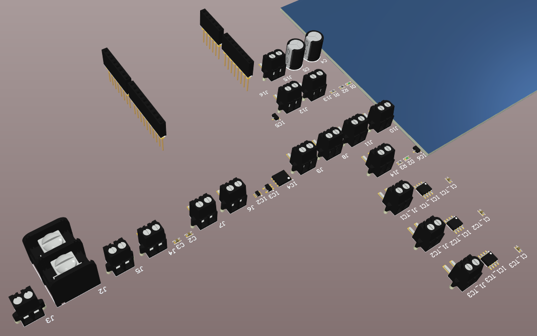
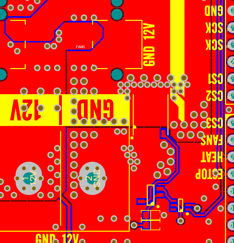
Board Layout and Design
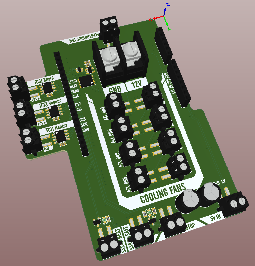
As usual, I transfer the components over to the PCB with an engineering change order, and we get to see the army of terminal blocks, and their barrier block general!
Thermocouple Channels
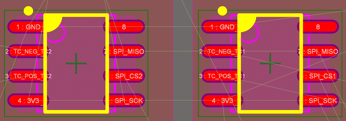
Before we get on with layout and routing, I wanted to show the difference between two thermocouple amplifier/converter ICs. You can see that by not using the REPEAT() function on the MISO and SCK pins, both ICs have the same nets on those pins, yet the SPI_CS is different for each one because of the REPEAT function. I also realized I need to fix the silkscreen on that footprint!
The thermocouples all get identical routing and layout quickly using the Copy Room Formats tool after laying out and routing the first thermocouple.
Board Shape
The STM32F746 Discovery board doesn’t have the same component layout as a typical Arduino/Clone/Nucleo board, so my board shape is a bit different than if I was building a shield for one of those boards. With an Ethernet connector on one side of the board, and an SPDIF connector on the other, and mounting posts/feet on the other side of the Arduino style connectors the area for a shield is constrained.
Because of these constraints, I have a small cutout on the left side of my board for the buttons and power source selection jumpers. On the right side my thermocouple inputs extend out over the microcontroller IC area, and the estop/solid state relay/power input extend off the end of the host board over the USB ports.
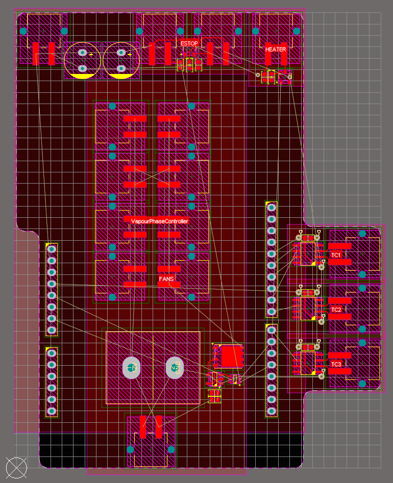
The electronics area cooling fan is over on the opposite end of the board, which should be flush with the host board. This will be at the top of the electronics area. The 12V power connector, MOSFET and bank of fan connection terminal blocks run down the centre of the board.
Optimizing the Board
The routing for the logic on this board is pretty simple, so I won’t waste time discussing that. There’s nothing high speed, impedance matched of really requiring any particular attention on the logic side of things.
Where things do get interesting is the fan power—with 18.4A of current to drive the 8 fans, it's not a huge amount of current, but it’s certainly not a tiny amount either. I designed the board with what I figured would be enough copper area, and it was so inadequate I wanted to show my failings and how I improved the design.
First, I’m using PDN Analyser to analyse the network. Normally I see it as just a verification I haven’t done anything stupid and in this case I’m glad I did simulate the design as it’s very likely the board would have failed early on in its life if I had left the design as is.
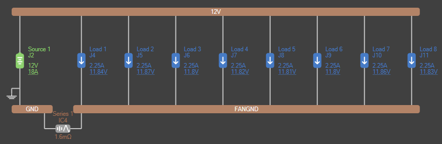
I’m only simulating the power going to the fans, from the large barrier block connector. Each fan’s connector is a separate load in the network, and the MOSFET is bridging FANGND to GND.
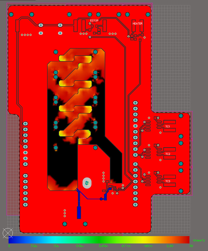
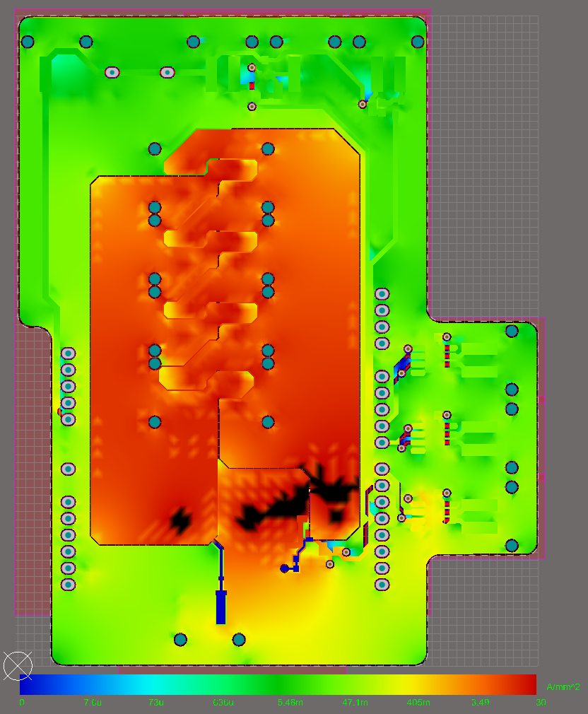
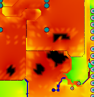
My initial simulation looks awful. This is showing the current density with the current limit set to 30A/mm2. For most boards, this would be a good upper limit, the black areas are anything over 30A/mm2 - the red for the rest of the board is just the top layer overlay. The actual current density in some of those areas is well over 200A/mm2, which would probably get hot enough to delaminate the trace from the board or potentially break the trace despite how wide it is, leaving me with no fans. Clearly this board’s copper area needs to be re-thought.
This is with the copper expanded to take up as much space as possible, I’m also showing the ground net too. I’m still getting some serious high current spots. The top layer alone will not be enough to carry the current for this board.
Adding a bottom layer and many vias is still not quite getting there. There’s going to be very high current density at the pins for the connector, and on the pins for the MOSFET unless I use thicker copper on the board, I can’t get away from that but I’d like to optimise the design further.
The main goal for me here is to try to get the same current density on the top layer as the bottom layer of the board in the same area. This means I’m fully utilising both copper layers to transfer current. One of the main snags you might encounter when doing this is adding too many vias. Vias remove PCB and copper where the hole is, so you can easily get into a position where you’ve added so many vias that you’re actually restricting the current flow and making things worse, because there is much less copper area for current to travel through.
Once I have a design which has equal, or close to, current on all copper layers, I’ll start removing vias in the direction of current flow to try to free up more copper area.
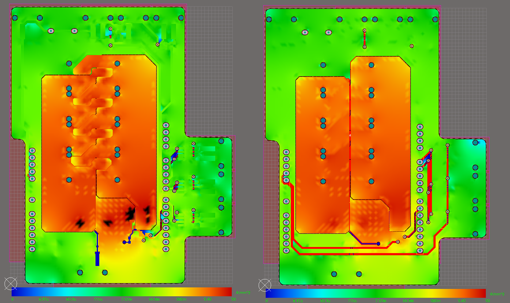
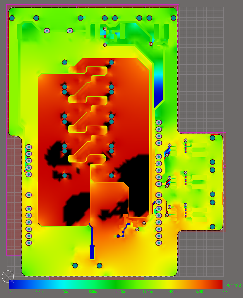
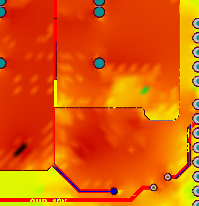
If I switch to a 50A maximum current view, you can see the top and bottom of the board is fairly well matched, I’ve removed most of the vias I originally had, opening up the area to the north of the MOSFET with vias only around the perimeter of the copper.
I was ready to call this optimal, to the point I added all my silkscreen and took screenshots of the completed board for this article.
I came back to the design the next day, unsatisfied with the component positions. The high current spots are certainly reduced, but it’s not really an optimal design for the FANGND net. Once again, I’ve found myself optimising an inefficient design. I had thought above moving the MOSFET when optimising the board, and should have done so at the time - but I had got myself fixed on this particular layout for no reason. I’ve mentioned this in articles and projects before, committing to a design that isn’t optimal, having come back the next day with fresh eyes I was able to see that I had committed to a poor layout and set about fixing it.
If I rotate the MOSFET, I can have the FANGND pins/pad facing the connectors with the GND pins facing the connector.
Initially, things looked much worse, the design was struggling to get current to the bottom layer. The necked down area of copper in the previous design actually added quite an advantage for getting power on both layers, as the copper area was so restricted. In the screenshots above, you can see the current density around the pad on the bottom layer is quite even, as the vias are conducting a lot of current very well.
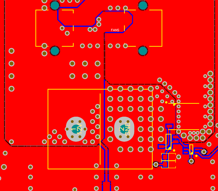
With 3 sides of the drain pads being exposed, I had a few more options than before. As I mentioned earlier, vias can really cut down on copper area, reducing current flow. For my optimised design, I am leveraging this fact to control where the current is flowing. In simulations, current was preferring to flow from the end of the MOSFET straight up the board, the path of least resistance, but the vias around the MOSFET were not able to conduct much current to the bottom layer. The current density on the top layer was much higher than the previous design’s combined top and bottom layer, so I knew that the design could be optimised.
I added a shield of small vias in the path of both the GND and FANGND nets to force the current to spread out, and also provide an optimal path for the ground net. There is almost double the copper area on the top layer for current to travel through than the previous design, despite my via barrier, but the vias are now able to conduct current to the ground.
With the maximum current density set to 30A, I still have a similar area of black where the current is exceeding the limit to the previous design but the current density on the copper layers, especially FANGND is 5-10A/mm2 lower. Yellow on the board is about 0.5A/mm2 as a reference point.
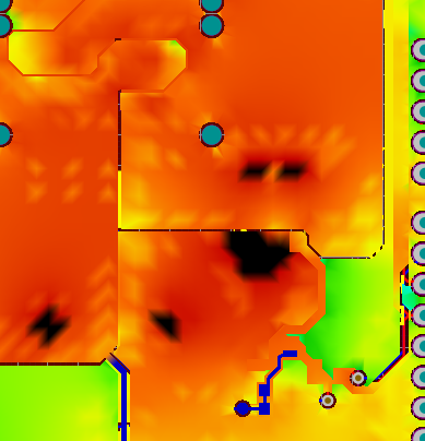
When looking at just the top layer with a 50A/mm2 current limit, we can see the black areas on the top are significantly smaller than the previous layout, and the overall shade of the board is lighter which signifies lower current density.
Finally
If you’d like to see some content on the build of the oven itself, or programming PID controllers leave a comment on the article. Otherwise, the oven’s source files and design will be available on my GitHub once I’ve finished the build, hopefully in a matter of weeks.
Despite the simple schematic for this project, it has been a reminder to me again not to get too fixed on a specific layout. The decision to place the MOSFET in that orientation was made very early on in the layout process when I was planning to place the terminal blocks differently. Once the terminal blocks were rearranged to their current layout, the justification for the MOSFETs location and orientation went out the window, but I was still mentally committed to it. I’m glad I went back the next day to move it - if you are trying to optimise a section of a design, it's always worth taking a step back and looking at the design as a whole to see if you can optimise the design at a higher level first.
As mentioned earlier, you can grab the Altium project and design files for this vapor phase reflow controller over on GitHub. It’s licensed under the MIT license, so you can do what you like with it.
Would you like to find out more about how Altium can help you with your next PCB design? Talk to an expert at Altium.