Copper Current Density for Simulations, The Quick and Dirty Way

In my previous article, PDN Analyzer Quick Start on a Motor Driver PCB, MattPVD asked the question, “How does one determine an acceptable current density?” I have to admit, I spent a lot of time trying to answer this exact question when I was first creating the simulation for the board. What current density is acceptable? The IPC have guidelines hidden away in their documents, but you have to pay to access those documents, which means it's not advice everyone can utilize.
In my mind, the current density of a trace mostly boils down to thermal constraints. This is exactly the same as in a high current integrated circuit; the limiting factor is most commonly going to be how hot it will get with the thermal dissipation and the load placed on it. This will be completely dependent on the specific implementation of the board, so unfortunately, I don’t think a hard and fast rule or set of guidelines is going to be optimal for any design.
Instead of writing about specific guidelines and how to use them, I want to tell you how I figure out a ballpark figure that should be acceptable for the design in question. Without using thermal simulation tools, such as Ansys IcePak, you won't truly know what your maximum current density should be. I see tools like PDN Analyzer as an incredibly effective means of determining whether your design is sane and going the right direction before moving on to real world testing and far more expensive simulation tools—if your design is pushing the limits.
Why Does Current Density Matter?
Simply put, current density is going to determine how hot the copper gets. A smaller area of copper will have higher resistance, and therefore a larger voltage drop as you run more and more current and generate more and more heat.
If your trace gets too hot, it could:
- Delaminate the board (cause the substrate to fail)
- Delaminate from the board (come loose)
- Cause thermal shutdown of nearby parts on the same copper conductor
- Melt/break the trace
- Greatly reduce the life of components on the board
None of these are desirable outcomes, so we want to ensure the current density on our boards is going to be within sane margins.
How Can We Determine the Maximum Current Density?
There are likely better ways to determine current density than this. However, if you are just checking the sanity of your design, this should give you a good enough value to work with.
If you know how much current you need to conduct through your PCB’s copper, what your maximum ambient service temperature is likely to be, and the maximum temperature your trace can reach, you can use the formulas from IPC-2221 to calculate the appropriate trace width. Ah, I hear you say, “Isn’t the whole point of this because we don’t have access to the IPC literature?” Well, thankfully, there are many online trace width calculators which have these formulas!
I’m using the calculator on the Advanced Circuits website, and because I’m not located in the U.S., Liberia, or Myanmar, I’ll be using metric for these calculations. You can use whichever units make you happiest.
For this example, I’m going to say we need to run 30A on the PCB, on an external layer. This external layer constraint is important for 2 reasons:
- Many PCB manufacturers use thinner copper on the internal layers,
- Internal layers are insulated by the PCB, and therefore will not cool down as effectively as external layers.
I want to simulate this board in PDN Analyzer, but to use the current checks offered by the software, I need to first know the current density. I expect my board to be used at a maximum service temperature of 45°C. You should consider how hot the inside of your enclosure will be if you are using one, and you should also take into account the climate of the various countries in which your board might be used. I want my maximum temperature to stay below 130°C, which is the glass transition temperature (Tg) of my board. The glass transition temperature is the point above which your board starts to get soft and will be far more likely to delaminate or fail. I’m also going to use standard 35μm thick copper, but if your board calls for it, you can get both heavier/thicker copper and higher Tg boards from most vendors as standard options.
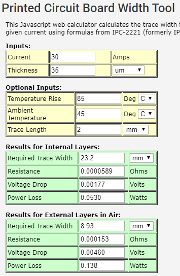
With this set of inputs, I’m going to calculate the absolute minimum trace width I could possibly use. Using this trace width will likely result in a short service life for the PCB, and will cause your product to fail in interesting and creative ways in service.
We can then use this minimum trace width to calculate the absolute upper limit of current density we want on the board. Simply multiply the trace width by the board thickness. Since this article is about the quick and dirty way, we’ll just use Google Calculator to do the calculation so we don’t have to bother with unit conversions.
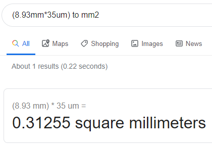
Simply search (8.93mm*35um) to mm2 on Google.
Now we know that we need 0.31255mm2 of copper area to conduct 35A if we want to heat the board up to its glass transition temperature. What we need for PDN Analyzer, however, is the current density in amps/mm2. Therefore, we simply divide the current we assumed by the area we calculated—so 35/0.31255—to get 111.98A/mm2.
This is, of course our absolute limit, and our design would be crazy to use it. If your design has anything over the current limit you calculate here, it probably needs a bit of rework.
How Can We Determine a Sensible Current Density?
If we want the product to survive long, we also need to figure out what sensible current density we want the vast majority of the board to meet. Some areas exceeding this current density are likely going to be fine, especially if they are surrounded by lots of lower current density areas. Remember that copper is a very good conductor of heat as well as current, so a small section of high current density may get hot, but it can also conduct that heat away to neighboring copper pours. I would be happy with the neck down of a trace going into an IC, for example, having a higher current density than we calculate here, as long as the rest of the trace is sensible.
Using the same method we used before to calculate the trace width, we can calculate our desired current density by just changing the maximum temperature rise to something a little bit more sensible. I’m going to try to keep all my traces below 65°C, it sounds like a good temperature and should keep connected ICs from getting too hot. With 45°C ambient temperature, this only leaves me with a permissible temperature rise of 20°C rather than 85°C we originally calculated!
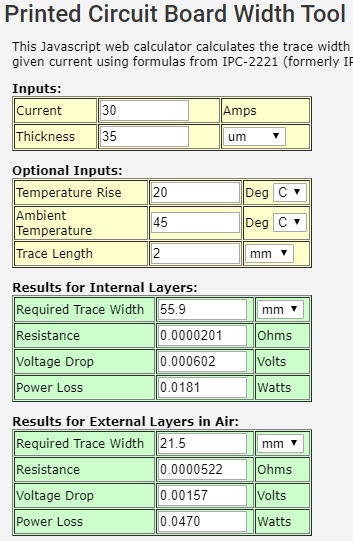
That’s a lot more copper! The total area is now 0.7525mm2, giving us a much more sensible 46.5A/mm2 to use for simulation purposes.
A Little Advice on Simulation
These numbers are going to vary, depending on your specific project needs. Don’t just use my numbers, as they may not be appropriate for your specific design.
Most of your fellow humans consider 55°C to be burning hot when they touch it! It's too uncomfortable for them to hold their skin against. If you do a lot of soldering, you’ll probably have a much higher threshold for considering something too hot. This is worth mentioning because if your product will have the conducting area you are designing exposed to human touch, you may want to consider keeping the trace temperature below 55°C so users don’t complain they are getting burnt from your product.
If you have large areas of your board just barely scraping through on current density, it’s likely to overheat. You need to make a judgement as to what balance of hot and cool areas of your board are suitable. If you simulate a board that has 30% of its area covered with a trace that will be 60°C under load, at 25°C ambient, your board itself is probably going to be close to 50°C overall with that load—so your ambient temperature may need rethinking.
If you have electrolytic capacitors connected to the copper area you are going to have higher temperatures on, you may want to check their datasheet for maximum service temperature, or lifespan derating at temperature. A cheap aluminium electrolytic capacitor that will last for years at ambient temperatures may only survive as few as 500 hours at 85°C. That’s less than a month, and your customers/users probably expect their device to last longer than that.
If you feel as though you are really pushing the limits with your simulation, you should do more extensive evaluation of your design in Ansys IcePak or perform extensive real world testing. A thermal camera and a can of black spray paint are cheaper than IcePak, but in real world testing, it may be harder to simulate a variety of conditions without expensive environmental chambers. Metals reflect thermal wavelengths, so in order to get an accurate reading, spray your entire board with black spray paint before testing it with a thermal camera.
Conclusion
My way of calculating an acceptable current density might not be for everyone, but it should give you an idea of whether your design is heading down the right path. The thermal implications of high current/temperature traces can be wide ranging for your entire circuit board and should be considered. Due to this fact, I wouldn’t recommend looking for a golden standard current density to stay below for all your PCBs.
If you are designing high power boards, your acceptable current density is likely to be far greater than that for a power distribution network that is supplying microcontrollers or logic devices.
Your device’s specific layout, operating environment, and enclosure options will greatly affect what current density is acceptable for your design. I hope this guide will help you determine what an acceptable limit is, so you can use a tool like PDN Analyzer to sanity check your design before prototyping it.