Current Monitor and Controller Project in Altium Designer
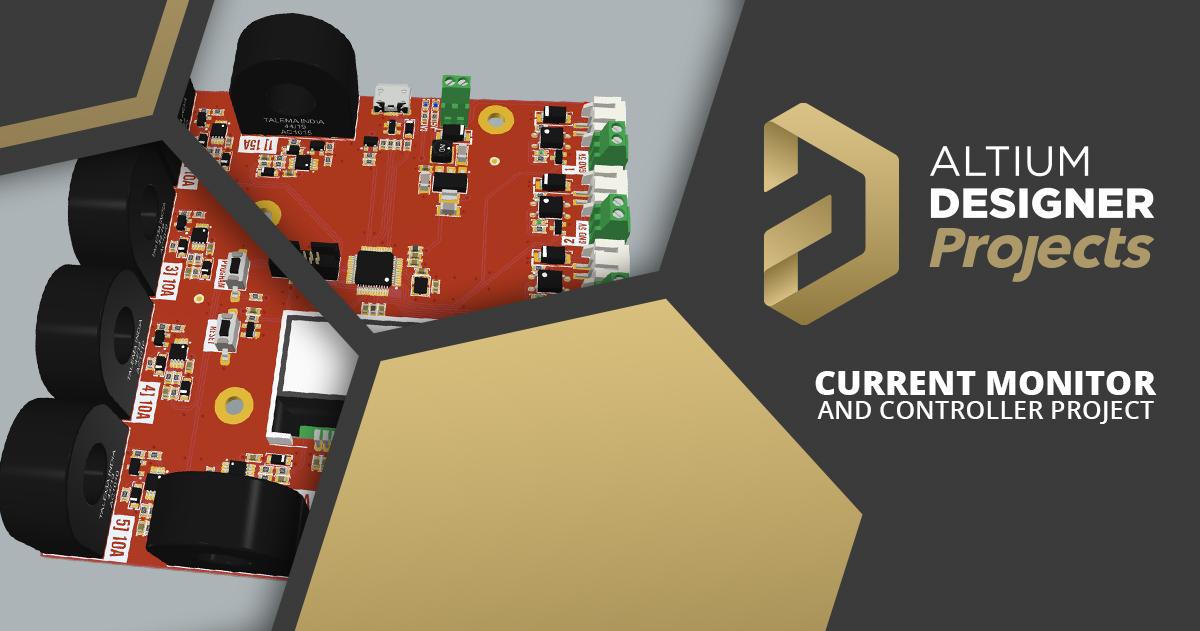
In a previous project, I discussed options for using Current Transformers, and built a single channel amplifier/precision rectifier for one. In this project, we’re taking that idea to new levels.
The house I rent has only 240V/16A to the garage. This is unfortunate, because as a Maker, I have some pretty fun toys in my garage, such as a CNC router and laser cutter. I have some moulds to machine for an upcoming big project in which I’ll be building some carbon fibre reinforced plastic parts. My old compressor trips the breaker to the garage instantly when turned on, so I’ve had to re-evaluate my options for running the CNC router—it needs more than the 16A I have available at full running load. Because of this, I bought a relatively tiny low noise compressor to reduce the current draw, but I need a way to make sure it won’t come on when the CNC router spindle is under high load, or when the spindle’s chiller is running.
My solution is to build a multiple channel current monitor, which will allow me to monitor the current draw of the router and associated equipment. This should allow me to determine when it’s safe to turn the little compressor on, depending on the other system loads. I need to have constant airflow to the tool-changing spindle as the bearings need to have air flowing through them to keep them clean, and the piston in the changer needs to apply constant pressure to the tool to ensure it doesn’t slip, so air pressure is vital.
I will have 6 output channels for the controller board to match the 6 current sense channels. I don’t need that many channels for my project, but as a generic open-source design, you might want to do something different with the board than me. I plan to have a display on the board as well, to show real time current.
This project is not a power meter. It doesn’t have any ability to monitor the voltage. Therefore, it also can’t monitor the power factor of the load either. My requirement is purely for trying to make sure I don’t trip my 16A breaker. If you need this functionality, this project could be a good starting point, as I will be adding a small transformer to isolate the AC voltage and dropping it to a more manageable level.
As usual with my projects, you can find the design files on GitHub; they are free to use under the very permissive MIT license. This allows you to use the project freely, as you wish. If you’re looking for the components used to build this project, you can find them all in my free and open-source Altium Designer Library®.

Above is the PCB design you'll be reading about in the Altium 365 Viewer; a free way to connect with your co-workers, clients, and friends with the ability to view the design or download with the single click of a button! Upload your design in a matter of seconds and have an interactive way to take an in-depth look without any bulky software or computer power.
Current Monitor Schematics
Despite the number of components on the PCB for this project, the schematics for this current monitor are rather simple.
Current Sensors
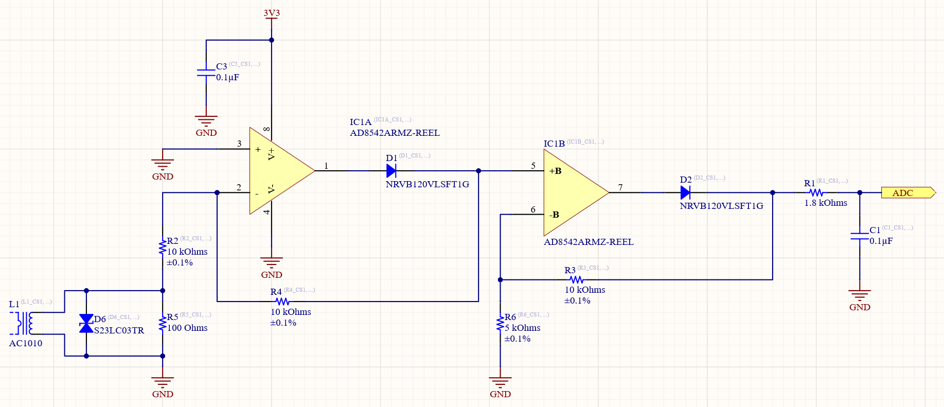
The current sensors are exactly the same as those I previously built, using the Talema current transformers. I have five 10A sensors with a 2:1 amplification of the signal, which, with rectification, gives four times the signal amplitude of the AC signal. The sixth sensor is a 15A with 1:1 amplification, which should allow the full amplitude of the 1800W tool changing spindle to be monitored. This is a standard, basic precision rectifier circuit. There are more advanced precision rectifier circuits that add a couple of extra components (such as a diode in parallel with the feedback resistor). For the purposes of this project, the basic circuit provides more than I require for accuracy and tolerance.
Microcontroller
The heart of this project is the microcontroller which will take all the readings from the sensors and determine which outputs should be on. I was looking seriously at the new STM32G series of microcontrollers, but ended up going with an NXP LPC11U35. The LPC’s main attraction for me is the USB bootloading functionality, allowing me to quickly deploy new firmware to the board once it’s installed in my CNC router’s cabinet. Nearly the entire LPC series allows the device to boot as a USB mass storage device with the onboard bootloader ROM, which allows new firmware to be copied into the USB drive that shows up on an attached computer, without the need for any additional hardware or software. This functionality will allow me to develop firmware in my office and to easily drop it onto the installed board.
The main drawback of the LPC11U35 is that it’s an older ARM Cortex and only features 10 bit ADCs. I need to check that the ADC will give me sufficient resolution for this project.
In the previous current transformer article, I forgot to get the RMS voltage of the signal out of the amplifier, and only captured the RMS voltage of the signal out of the current transformer.
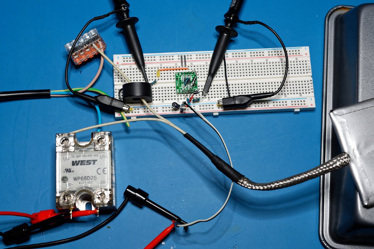
I rebuilt the current transformer circuit on a breadboard to get some new scope readings. I’m using a solid-state relay triggered by my benchtop power supply to switch on the 1.1kW ceramic heater that’s sitting on an upside down baking pan for thermal isolation from my bench.
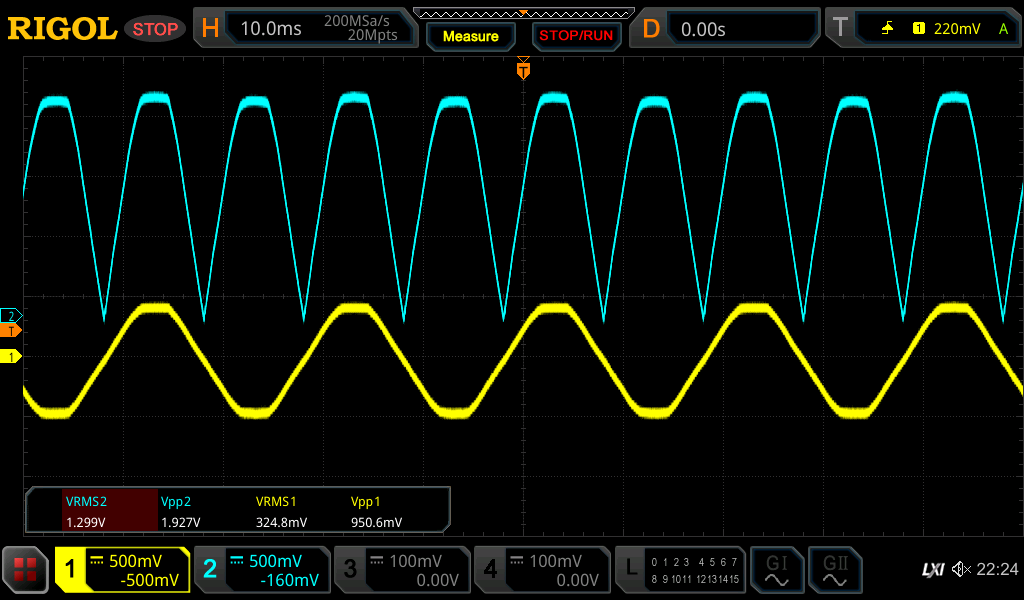
The blue trace (channel 2) is the output of the precision rectifier, and the yellow trace (channel 1) is the AC output from the current sensor prior to the opamp.
With the current sensor amplifier built as per the circuit in this project, I have 1.299v RMS with a theoretical 4.429A flowing through it. This gives me a resolution of about 293mV per amp. With a 10 bit ADC (1024 values) and a 3300mv range (3.2mv resolution), this gives me a readable resolution of about 0.01A, which is not amazing compared to the 14 or 16 bit ADCs in more modern microcontrollers, but still sufficient for this project, and many other applications too.
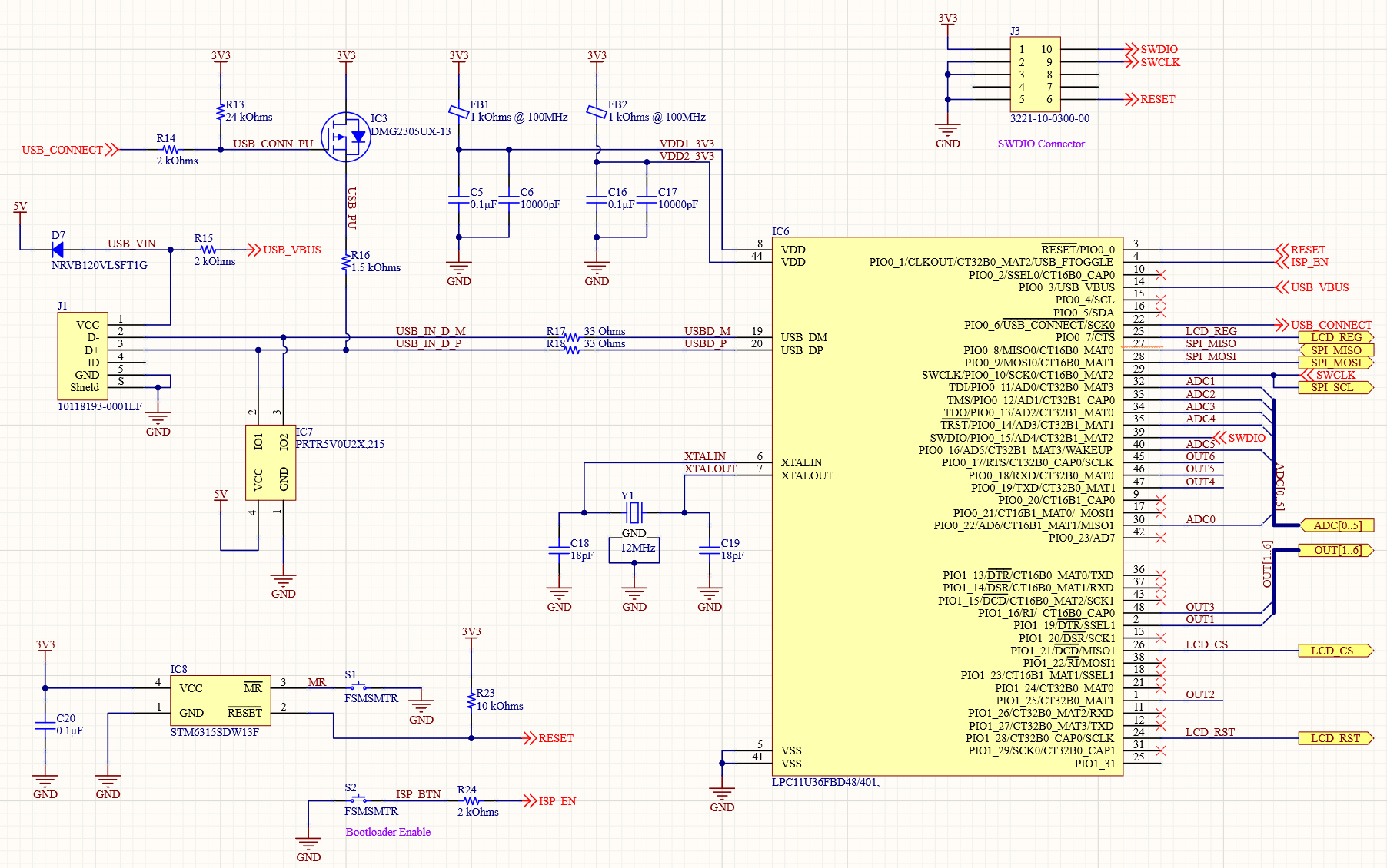
There’s a lot going on in this one schematic sheet! It’s worth noting right away that the pull-up P-Channel MOSFET on the USB line isn’t required for the latest silicon revisions for the LPC11U series, but I’m going to leave it in because I have some older MCUs on hand that I might use for populating this board and don’t want to get caught without my USB connection working. If you are buying new stock of the LPC11U35, you can do away with everything associated with IC3.
While we’re on the topic of USB, I also have a TVS diode that’s designed for protecting USB 2.0 lines from ESD events. USB connectors are a great location for an ESD discharge directly into the microcontroller, so they’re my top priority for protection.
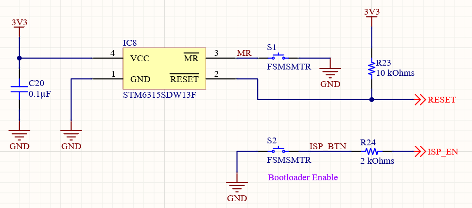
As we continue down the left side of the schematic, I have a reset supervisor IC to ensure that the 3.3V supply is stable prior to booting the MCU, with a button to manually reset the board. I also have the bootloader enable button with it, as I like to keep things together logically. To take the board into the USB mass storage bootloader mode, it’s a simple matter of holding down the programming button S2 and then pressing the reset button S1. Holding the programming button down for a second or so after boot will boot the device into a USB mass storage client device if the USB cable is connected.
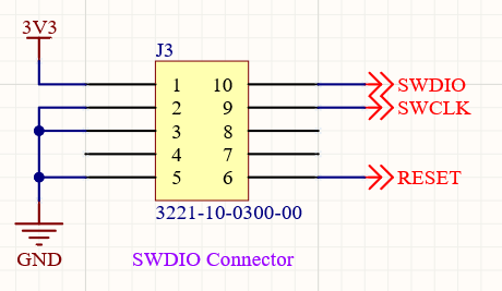
In the top right of the schematic, I also have a standard 10 pin single wire debug (SWD) connector to allow the board to be debugged in an IDE.
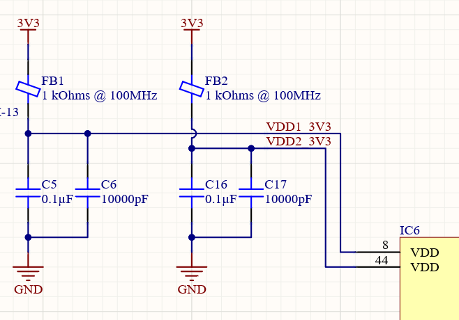
Finally, the input filtering for the microcontroller. We’ll get to the IO connectors in a later section of the article, so don’t worry that I’ve skipped over the two buses and how to set them up! The power filtering for this board is fairly critical, as it will be installed in—and powered by—an industrial machine that generates a large amount of electrical noise (both conducted and radiated). There are over 2000W of AC-DC supply, a 2200W Variable Frequency Drive running a spindle, DC servos, an industrial chiller, and a dust collector, all running off the same AC supply. Due to the amount of noise, I’m putting a ferrite bead close to each power pin with two decoupling capacitors—normally in a microcontroller design I would have just the one ferrite and perhaps a couple of bulk capacitors, but for this design I want to have the shortest traces possible between the microcontroller and filter. As the microcontroller power supply pins are on opposite sides of the device, I chose to build a filter for each pin to keep the tracks short.
The ferrite for each power pin was chosen to have as high a resistance as possible at 100MHz, while having the lowest DC resistance possible. Basically, I tried to determine how much DC resistance I was willing to live with, and then maximized the resistance at frequency for that DC resistance.
Power Supply
My CNC router already has multiple supplies I can choose from, the 5V rail is the cleanest and least utilized, so it makes sense to run the board from this supply. As a bonus, it will also allow me to run the board from a USB cable on my workbench. As I only ever expect one of these supplies to be powering the board, I have added a simple diode to each input to act as reverse polarity protection and basic protection against both supplies being plugged in at once.

The protection diode was chosen for a low forward voltage drop to ensure a very low cost linear regulator could be utilized without the combined voltage drop of both devices taking the output below the 3.3 volts I require.
Between the linear regulator and the protection diode, I have added a pi filter. I don’t know exactly what frequencies I will be dealing with on the input, so I aimed for the highest inductance possible within the 4-5mm sized inductors available. I’m using a shielded ferrite core wire wound inductor to get the lowest DC resistance I can, as this board could potentially pull up to 1 amp with all the LEDs and Optoisolators powered. With the current requirement and size known, it was just a matter of looking for a high inductance value with a low DC resistance inductor that also met the size and current requirements. I threw a 10uF cap on either side of the inductor to complete the pi filter, with this being a low cost value that still has a decent amount of capacitance.
Current Monitor Outputs
I probably don’t need to optoisolate each output, as the solid state relays I use have optoisolators built in, but being an open source design I don’t know if perhaps someone will connect a relay or an industrial controller’s IO directly to the board. As an added bonus, the isolator gives me peace of mind. The current for the LED in the isolator is higher than the ARM Cortex can drive, so I have a very cheap N-Channel MOSFET to drive the LED in the optoisolator and an external one that can be seen to indicate the output is enabled.
I also only actually need two outputs for my use on this board design, but I figured as an open source project it’s probably nice to have this be a more generic design. I’m adding 6 output channels to match the 6 current sense channels, so if this were to be used in a different industrial machine, it would allow the controller to enable or disable each load for which there is a current sensor.
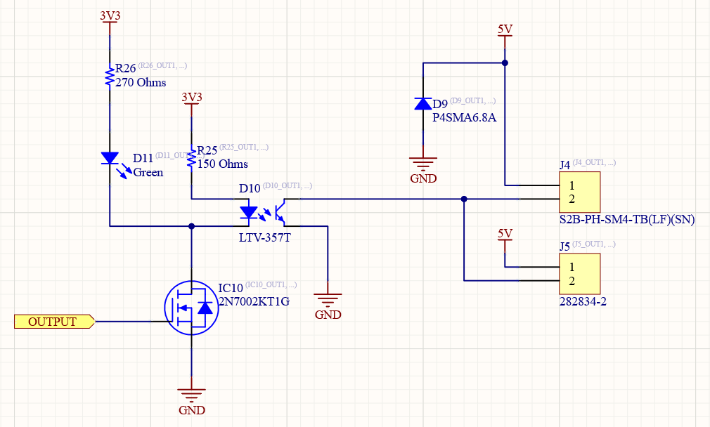
I also have a TVS diode that is as close to 5V as I could get to protect the board from ESD on the input connectors. I’m planning to use some pre-crimped JST KH connectors from DigiKey to connect my solid state relays to this board, which are JST PH compatible. I also added a 2.54mm pitch wire-to-board terminal block to the board as well, to provide added flexibility for other applications. The pre-crimped wires are great for me, as I can cut one in half and wind up with two cables, ready to use with the solid state relay, preventing me from having to cut lengths of wire and strip two ends—potentially saving me seconds in installation! In all seriousness though, the crimped connectors are going to be more secure and less likely to come out or fatigue on a machine that has a lot of jolting and vibrating.
Display
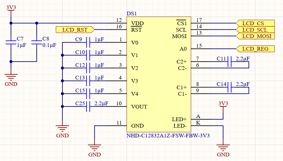
The final schematic block of this project is the LCD display. I decided to use a relatively inexpensive and robust Newhaven graphics display, as they have a simple SPI interface. I was very much hoping to use a 128x64 pixel sized display, but the board just didn’t have room, so I came back to the schematic during board layout and changed the design to use a 128x32 pixel display. It needs lots of decoupling capacitors, but otherwise has very little in the way of connectivity requirements.
Multichannel Design with Altium Designer
One of the key aspects of this project is that I have five identical current sensors channels and six identical output channels, making multichannel design ideal for this project. In my opinion, this is something that Altium greatly excels at compared to other ECAD software I’ve used. Its features allow the rapid routing and layout of the board and easy to read schematics.
Rather than duplicating schematic sheet blocks on your top level sheet, as shown below, I can make the schematic much cleaner just adding one schematic sheet block and using the REPEAT function on it.
.png)
This takes all of those schematic blocks and turns them into one virtual stack of components. For this project, it allows a single connection from the microcontroller to all the current sensors. If I need to change the ports on the schematic symbol block, the changes will be applied to all of the channels at once, saving time if my project needs change during the design phase.
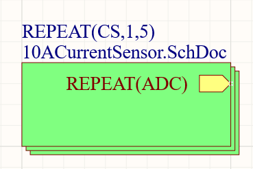
By using the repeat function, I now have all our sensor channels grouped together making the schematic easier to read, and it will make the PCB layout far easier when I get to that point of the project.
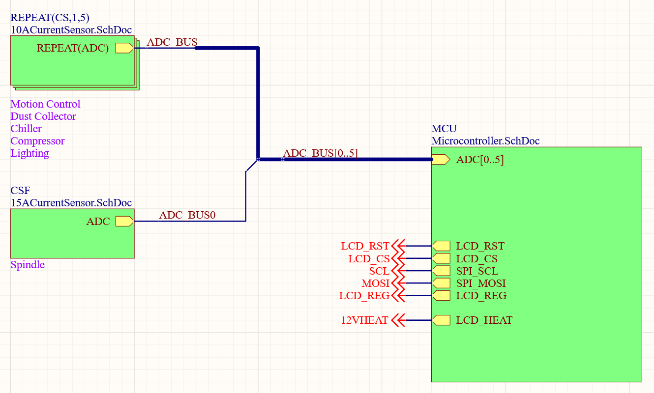
Let’s go through how to take advantage of this feature and use it in your design.
Using Busses
For the multichannel tools to work you need to use buses to bring your connections for the channels together. In our microcontroller schematic, rather than having a port for each ADC connection we will have a single port for all the connections.
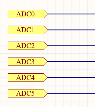
This makes your schematic cleaner, not requiring you to have all 6 ports broken out.
You can use Place -> Bus from the main menu to place a bus rather than a wire. You can think of a bus as a bundle of wires together. To make the bus work, you need to tell Altium how many connections are running on the bus. This is done by placing a net label (Place -> Net Label) on the bus, and giving it a name such as ADC[0..5]. This means the bus will carry ADC0, ADC1, ADC2, ADC3, ADC4 and ADC5, the double dots in square brackets meaning “from 0 to 5”.
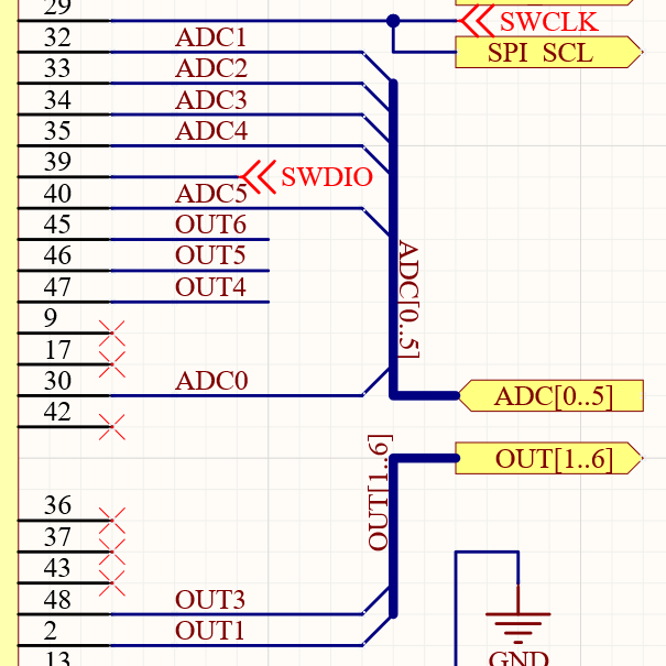
When using the repeat function, you will need to have your net numbering start at 1 rather than 0. For the ADCs however, I have the 15A current sensor as well which is not part of the repeated block, and therefore I’m starting with 0. ADC channel 0 will be for the 15A sensor, with 1 to 5 for the 10A channels. The OUT bus is numbered 1 to 6, as each of those will be a repeated block on the schematic and board.
After naming your bus, you will also need to add a net label to each wire that is going to the bus. The wires should have the same name as the bus, with the connection number at the end. For example, OUT1 and OUT3 are joined to the bus OUT[1..6]. These wires connect to the bus with a Bus Entry (Place -> Bus Entry), which is the 45 degree angle connection you see. You might also notice that OUT4, OUT5, and OUT6 are not actually connecting to the bus wire graphically - the name of the net is enough for Altium to know that these wires will be running in the bus. This is very convenient and saves from the schematic getting unreadable where all the wires would need to cross over each other.
Multichannel Schematic Blocks
Now that the microcontroller sheet is set up with the relevant ports, we can add it to a top-level schematic sheet. The easier way to do this is not to use Place -> Sheet Symbol, but instead to right-click your schematic and go to Sheet Actions -> Create Sheet Symbol From Sheet. This will create a symbol for the schematic as well as add all the ports you have in the schematic, saving time.
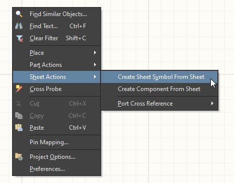
Do the same thing for your channel sheet, so you now have both sheet symbols in the schematic. The output channel sheet now needs to get renamed, the format is:
REPEAT(name, start, end)
By default, each component in the channel will be named ‘designator_sheetname’. Personally, I like having the designator first for being able to quickly read the bill of materials to see what type of component the line is for—but if you prefer a different format there are a number of options available Project -> Options -> Multi-Channel window. If you’re still not happy with the format, you can even enter in your own designator format using the variables from the standard options.
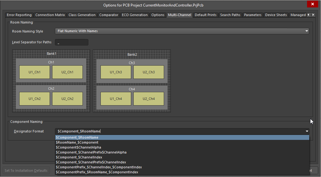
It’s very important that you also wrap your port name in REPEAT( ) as well, or the wire will connect only the first bus entry to every port, rather than generating a new port for each channel. Generally, the exception to this is for communications protocols, where you might want the same SPI Clock/MISO/MOSI or I2C SCL/SDA going to each sheet. This gives you a lot of flexibility for how the multi-channel sheets can be used.
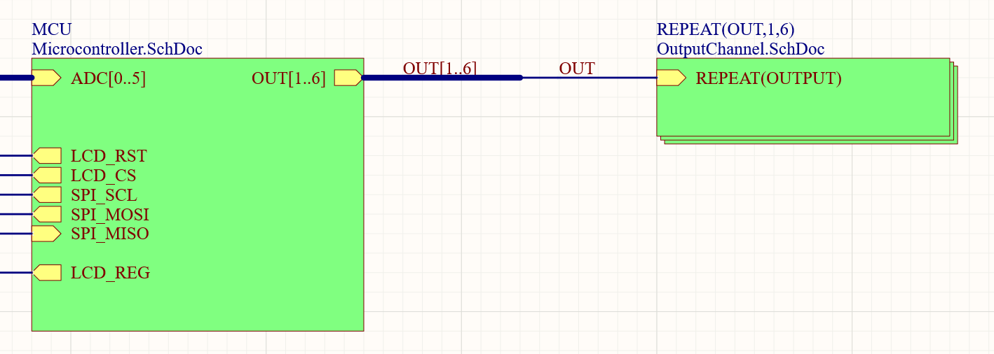
Now it’s a simple matter of having a named bus coming from the microcontroller bus port, and then directly connecting to a wire with the same name as the bus. It might look a little odd, but it tells Altium that you want to break the bus out to each of the schematic sheets. Altium will automatically add the channel number to the end of the bus net name as it generates each channel. The bus name does not need to match the port name, or the name of the bus in the schematic sheet the block is for. It can be the same or different—the only naming that matters is the bus and the wire.
.png)
I have applied the same set up to the current sensors, as I mentioned earlier in the article I have numbered the ADC bus from 0 to 5, as I’m breaking out ADC0 for the 15A sensor with a Bus Entry.
Current Monitor PCB Layout
Now that the multi-channel schematic is complete, I can start the board layout. It’s as simple as the top level schematic looks, as I only need to route the first channel for each of the repeated channels.
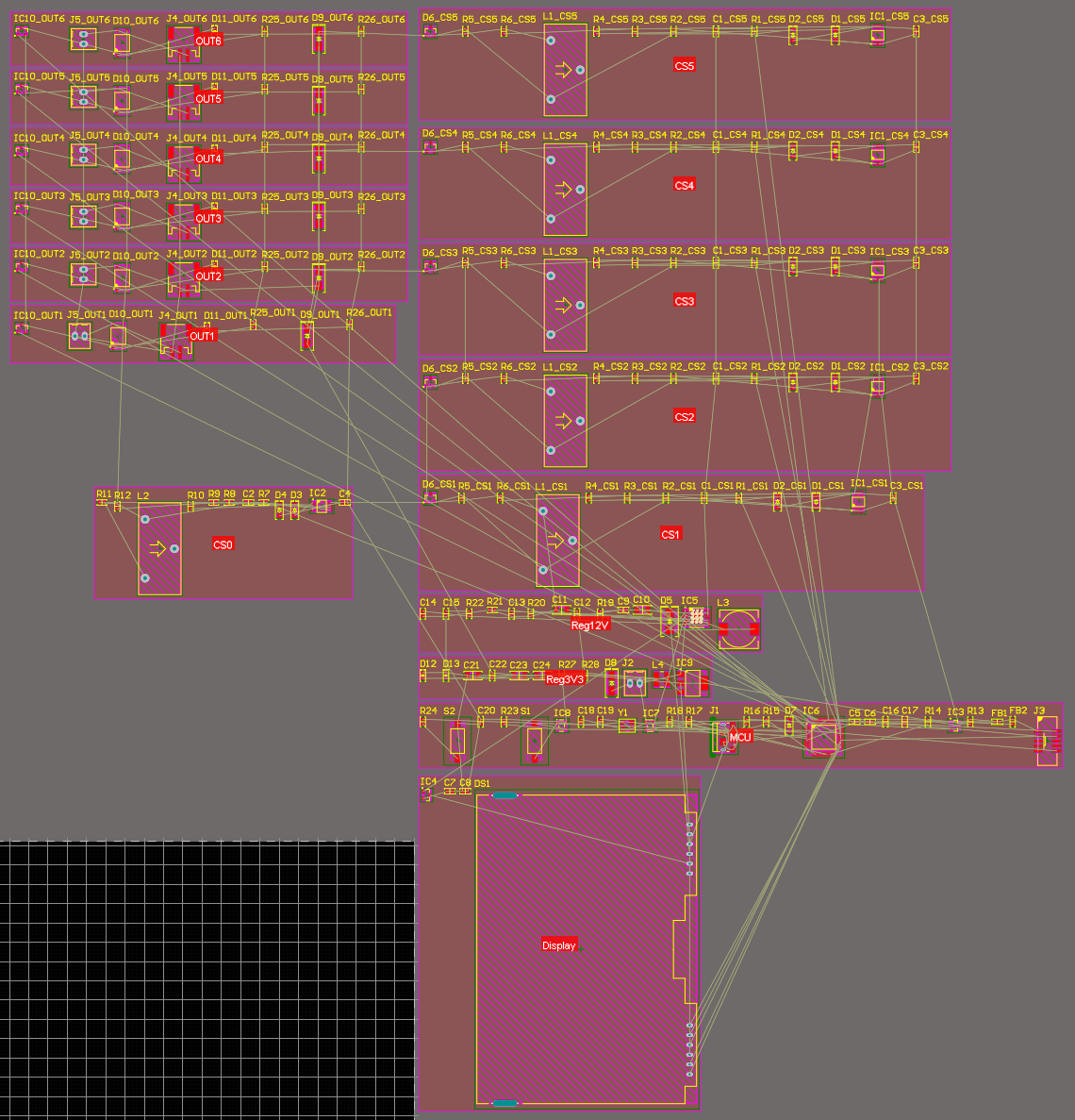
Once I execute the engineering change order to add all the components to the PCB, you’ll see all the top level sheet blocks in their rooms. Worth noting here is the multiple unrouted nets reaching out to the channels from the microcontroller showing that all my bus naming worked well, as each channel is connected correctly. If I had not added the REPEAT( ) command to the ADC and output pots, we would only see one wire going up and then connecting in parallel. The same as the power connections.
You might also notice the footprint for the display looks pretty large. This is the 128x64 pixel display I mentioned earlier which I was hoping to use. After routing the board and not being able to fit it on the PCB I changed it for the 128x32 pixel display seen in the schematics.
I’m starting out with the output connection. I’m going to route the first channel inside its room with everything required except the external connections. I have also reduced the room to a more practical size for the arranged components.
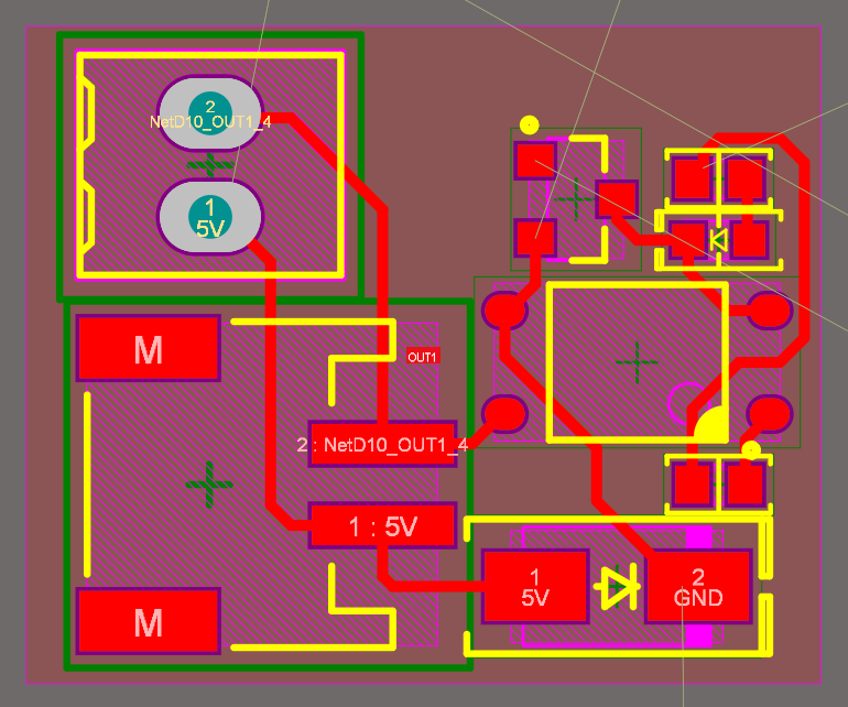
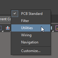
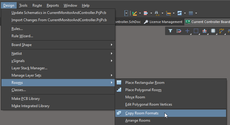
Now I can save a huge amount of time by using the Copy Room Formats tool. There’s two main ways to get to this tool, firstly if you have the Utilities toolbar enabled; it’s under the rooms icon.

You can enable the Utilities toolbar by right clicking anywhere at the top of the designer window and checking Utilities.
The ‘long’ way to reach the tool is through the top menu, by going to Design -> Rooms -> Copy Room Formats.
Once the tool is active, it’s a simple matter of clicking the first room that you have already routed (your template), then clicking on the next room you want to have the same layout and routing.
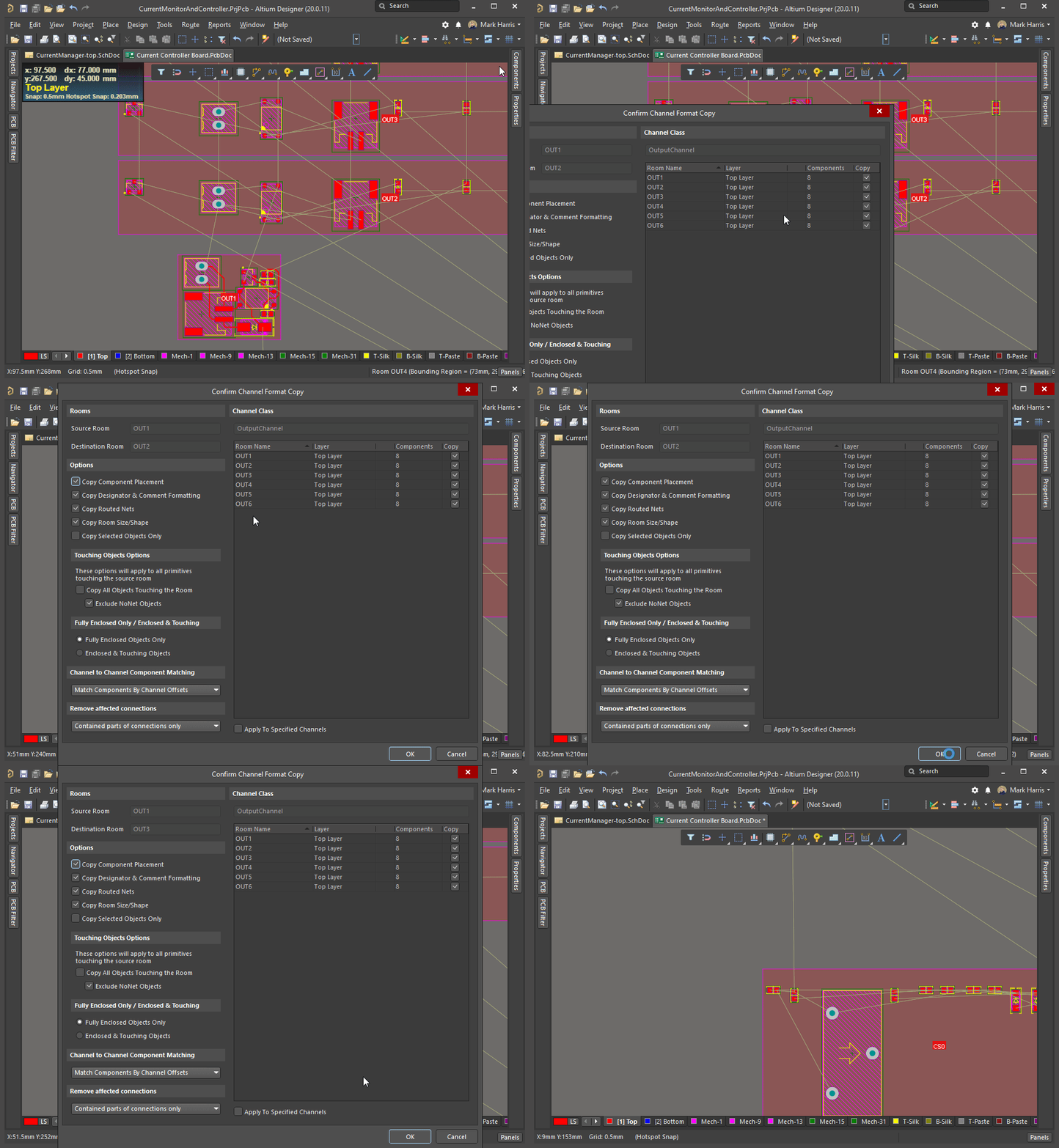
You can continue clicking on additional rooms to apply the same settings to those rooms too. The tool only works for rooms that are in the same multi-channel set. This means I can’t apply the format from a multi-channel ADC room to the 15A ADC. While the 15A ADC is almost the same schematic and only varies by one resistor value, it’s not compatible as it was not in the same multi-channel set as the others.
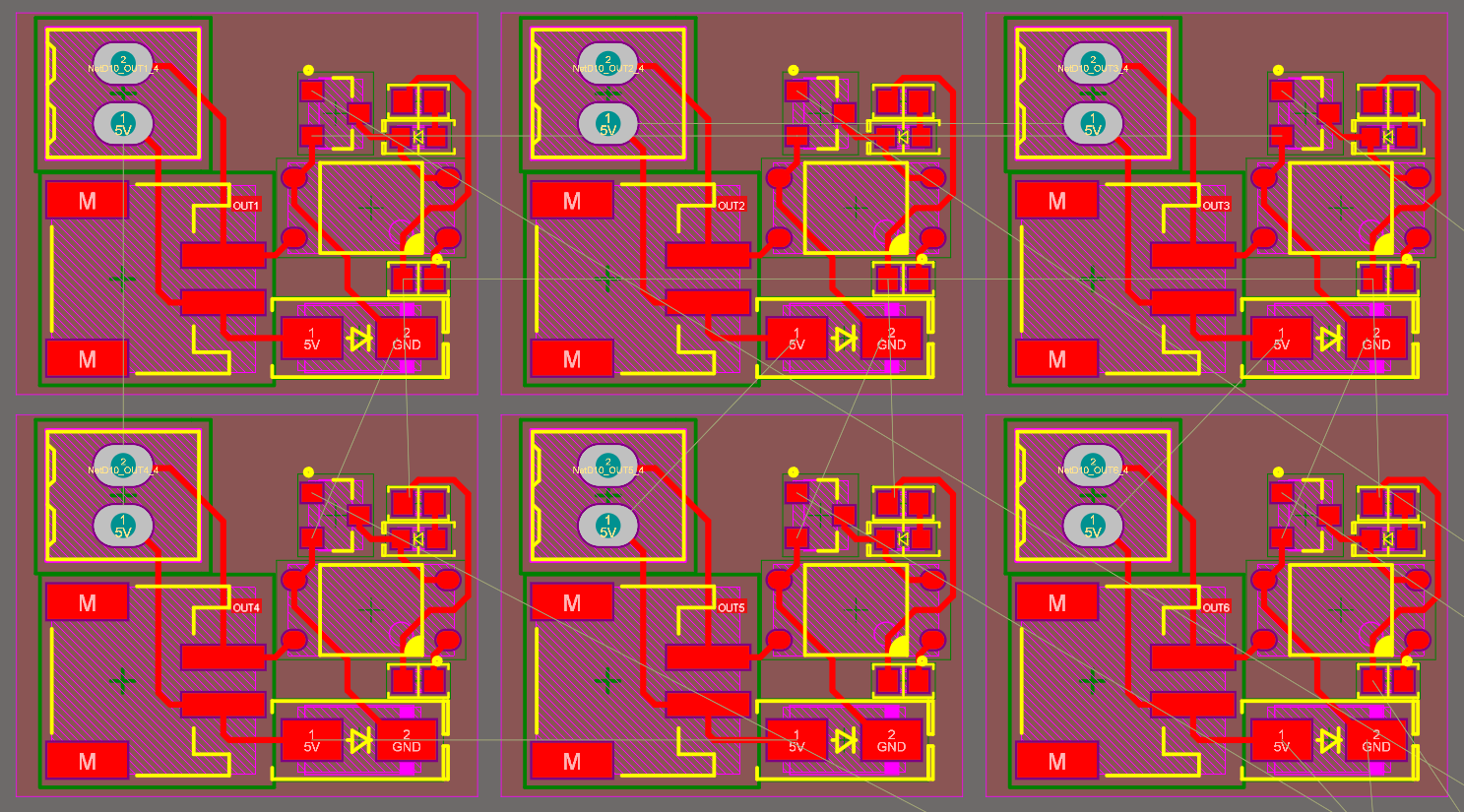
After I’m done with copying the room formats for the output channels, I have 6 identically routed channels for the output. The schematics and routing for each channel in this design are very simple, but I’m sure you can imagine how much time this will save with a complex multi-channel audio product or advanced multi-channel sensor.
I applied the same technique to the ADC channels, resulting in the vast majority of my board routing already being complete.
I’m planning on using a low cost Chinese PCB supplier, as they offer the best price for a 100mm x 100mm board. With this size constraint to work with, I can layout all the channels. I was able to fit all the outputs down one side of the board, but the current sensors, despite their small size, are still too big, and therefore I’ve placed them in a U shape around one side of the board.
I’ve placed my USB connector and 5V input close to each other on one edge of the board as well to keep the power routing tidy. Given that this is a two layer, 1.6mm thick PCB, I decided not to run impedance matched traces for the USB lines to the microcontroller. Given the data rate that the USB boot loading or serial port will use, signal integrity isn’t going to be overly critical. I’ve connected this microcontroller to a USB port with wires soldered to the microcontroller pins, and then a USB connector directly, so I know it will cope fine with this mistreatment. For a 2 layer 1.6mm thick PCB, my USB traces would have to be around 1.5mm wide to be impedance matched, and that's a little awkward for routing.
Finally, I have the screen mounted somewhere that hopefully, it won’t have too much in the way of cables blocking a view of what is displayed.
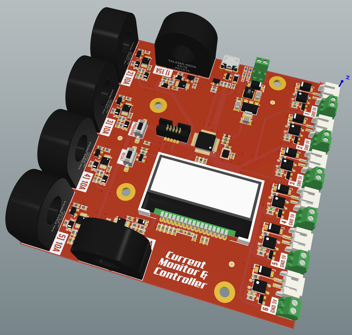
I’ve added some mounting holes to the board, as well as fiducials. The mounting holes are vital for this board as it will be mounted vertically in an odd place within my control cabinet.
With a little bit of fun for some artwork, the board is looking pretty good. The font ‘AlternateGothic2 BT’, which I have on my computer for some reason, looks really great for labeling the connectors. It’s legible and very compact which is great for the terminal blocks.
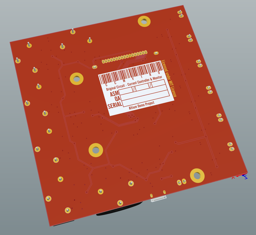
On the bottom of the board, I’ve added a fairly standard block for designs I work on for clients, having a barcode for tracking or loading test programs for a generic fixture, assembly date, QA section, and an area for a serial number. I like the way that this block finishes off the bottom of a board and makes it look a little more classy.
Finally
The board for this current monitor has been built to be a fairly generic current sense and control board, despite my rather specific requirements. The design files are licensed under the MIT license, so you can make your own or base a section of your own project on the design if you wish. As always, you can find the project design files over on GitHub.
Altium Designer on Altium 365 delivers an unprecedented amount of integration to the electronics industry until now relegated to the world of software development, allowing designers to work from home and reach unprecedented levels of efficiency.
We have only scratched the surface of what is possible to do with Altium Designer on Altium 365. You can check the product page for a more in-depth feature description or one of the On-Demand Webinars.