Design Basics for HDI and Planning for the HDI Manufacturing Process
As the world of technology has evolved, so has the need to pack more capabilities into smaller packages. PCBs designed using high-density interconnect (HDI) techniques tend to be smaller as more components are packed in a smaller space. An HDI PCB uses blind, buried, and micro vias, vias in pads, and very thin traces to pack more components into a smaller area. We’ll show you the design basics for HDI and how Altium Designer® can help you create a powerful HDI PCB.
ALTIUM DESIGNER
The best PCB design application for HDI PCB manufacturing.
High density interconnect (HDI) printed circuit design and fabrication started in 1980 when researchers started investigating ways to reduce the size of vias in PCBs. The first production build-up or sequential printed boards appeared in 1984. Ever since that time, designers and component manufacturers always look for ways to pack more functions on a single chip and a single board. Today, HDI design and fabrication are codified in the IPC-2315, IPC-2226, IPC-4104, and IPC-6016 standards.
When planning an HDI PCB design, there are some design and manufacturing challenges to overcome. Here is a short list of challenges you may run into when designing an HDI PCB:
- Limited board workspace area
- Smaller components and tighter spacing
- Larger number of components on both sides of PCB stackup
- Longer trace routes creating longer signal flight times
- More trace routes required to complete the board
With the right set of layout and routing tools built on a rules-driven design engine, you can violate the normal rules in PCB design and create powerful PCBs with very high interconnect density. Working with high-density PCB routing and fine pitch components is easy when you use advanced PCB design software that is built for HDI PCB design. You can create your new HDI design and plan for the HDI manufacturing process with the world-class design features in Altium Designer.
What’s Different About High-Density Interconnect Boards
The HDI manufacturing process differs from the traditional PCB manufacturing process in a few simple yet important ways. The use of thinner traces, smaller vias, more layers, and smaller components can still be easily accommodated in your design software, but design for manufacturing (DFM) requirements become more difficult to accommodate. The exact DFM requirements depend on the manufacturing process and materials used to build the board. DFM requirements also become important when we consider reliability requirements.
Material selection needs to answer these questions:
- Will the dielectric use chemistry compatible with current chemistry used by core substrate material?
- Will the dielectric have acceptable plated copper adhesion? (Many original equipment manufacturers [OEMs] want >6 lb./in. [1.08 kgm/cm] per 1 oz. [35.6 µm] copper.)
- Will the dielectric provide adequate and reliable dielectric spacing between metal layers?
- Will it meet thermal needs?
- Will the dielectric provide a desirable “high” Tg for wire bonding and rework?
- Will it survive thermal shock with multiple SBU layers (i.e., solder floats, accelerated thermal cycles, multiple reflows)?
- Will it have plated, reliable microvias?
There are nine different general dielectric materials used in HDI substrates. IPC slash sheets like IPC-4101B and IPC-4104A cover many of these, but many are not yet specified by IPC standards. The materials are:
- Photosensitive Liquid Dielectrics
- Photosensitive Dry Film Dielectrics
- Polyimide Flexible Film
- Thermally Cured Dry Films
- Thermally Cured Liquid Dielectric
- Resin Coated Copper Foil (RCC), dual-layer and reinforced
- Conventional FR-4 Cores and Prepregs
- New ‘spread-glass’ laser-drillable (LD) Prepregs
- Thermoplastics
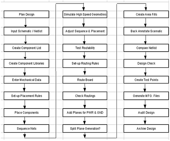
The HDI PCB design process is shown below. Routing efficiencies for HDI are dependent on stackup, via architecture, parts placement, BGA fanout, and design rules. The most important parts of planning your HDI layout are to consider your trace width, via size, and placement/escape routing for BGA components.

General overview of the HDI PCB design and layout process.
Always check with your board house to determine their fabrication methods for HDI PCB manufacturing. You’ll need to determine the limits of their fabrication methods as this will influence the feature sizes you can place in your layout. The ball pitch on BGA components will determine the via size you need to use, which then determines the HDI manufacturing process required to create the board. A central feature of your HDI PCB is microvias, which need to be precisely designed to accommodate routing between layers.
Microvia Design for HDI PCB Manufacturing
Microvias need to be carefully designed to ensure they can be reliably fabricated with mechanical or laser drilling. The exact HDI manufacturing process depends on the aspect ratio and diameter of the via. This will also determine the cost of drilling per via.
- Via-in-pad designs can be plated over in a design process known as VIPPO.
Learn more about the advantages of VIPPO design for microvias.
- Another method for increasing routing options is placing vias in pads. As long as you maintain a clean electrical connection, you can place vias directly in pads and drop the connections to other layers.
Learn more about designing laser-drilled via-in-pad connections.
- New interconnect designs and architectures are being developed and improved for more advanced HDI designs.
Learn more about other interconnect options for HDI PCB manufacturing.
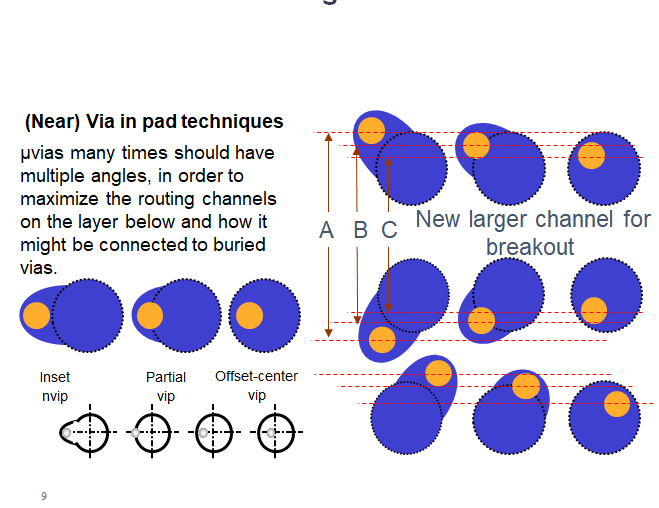
With the right set of HDI PCB design tools, you can easily create the microvias or via-in-pad design you need to mount and route your components. With the right set of powerful CAD tools, you can easily create via designs that comply with your manufacturer’s DFM requirements. You’ll have the tools you need to create the via designs shown in the figure below.

Via-in-pad design styles for HDI PCBs.
Routing your HDI PCB is quite easy with the right set of design tools. You simply create an impedance profile and define your desired trace width while keeping your manufacturer’s DFM guidelines in mind. With the right PCB design tools, you can define all DFM requirements for component spacing, trace clearances, and vias as design rules, which are then used to examine your PCB layout as it nears completion.
HDI PCB Manufacturing Processes
There are a number of steps involved in the typical PCB manufacturing process, but HDI PCB manufacturing uses some particular steps that are not used in other boards. These steps involve formation of traces and vias in each layer. This consists of the following steps:
- Photoresist deposition and exposure: This is used to define areas to be etched, which will leave behind a pattern of conductors on the laminate.
- Etching and cleaning: The current industry standard etchant is a ferric chloride solution. After etching, the leftover photoresist can be reclaimed and the resulting conductor pattern is cleaned.
- Via formation and drilling: Vias need to be defined using mechanical or laser drilling. For high via density, the via holes can be removed chemically.
- Via metallization: Once vias are defined, they are metallized to form a continuous conductive interconnect.
There are four via metallization processes that are used in HDI manufacturing. These methods are:
- Conventional electroless and electroplating copper
- Conventional conductive graphite or other polymers
- Fully and semi-additive electroless copper
- Conductive pastes or inks
Larger vias can be drilled, but the costs eventually exceed laser drilling costs with lower throughput as a slower drilling speed is required. Laser drilling is by far the most popular microvia hole formation process, but it is not the fastest via formation process. The chemical etching of small vias is the fastest, with an estimated rate of 8,000 to 12,000 vias per second. This is also true of plasma via formation and photovia formation.
In laser drilling, a high fluence beam is used to place a hole in a PCB laminate. Lasers are capable of ablating dielectric material and stopping when intercepting the copper circuitry, so they are ideally suited for creation of depth-controlled blind vias. The wavelengths for laser energy are in the infrared and ultraviolet region. A beam spot size as small as approximately 20 microns (

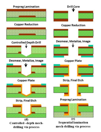
Microvia drilling and metalization processes in an HDI manufacturing process.
Design Your Feature Size to Satisfy HDI DFM Requirements
Although DFM requirements for an HDI manufacturing process are quite stringent, the number of different available processes give you some flexibility to design the board you want. Your design tools are critical for designing your HDI circuit board to satisfy these DFM requirements.
- Not only are microvias different in size, but the fabrication process is different compared to through-hole vias.
Learn more about microvia manufacturing techniques in the HDI manufacturing process.
- The HDI manufacturing process used for microvias depends on the via diameter.
Learn more about using mechanical and laser drilling for HDI vias.
- Laser-drilling is more common in advanced designs with high layer count, and you’ll need to design your board such that it can be manufactured with your fabricator’s laser system.
Learn more about how ultrafast lasers are used in the HDI manufacturing process.
Getting Your Board into the HDI Manufacturing Process
Once you’ve finished your HDI PCB layout and it’s passed important DFM checks, it’s time to prepare deliverables for your fabricator and assembler. Your deliverables are standardized documents that ensure your new board can be produced at scale and with a high yield. These documents also give you a chance to help your fabricator source components for your HDI PCB.
The unified design environment in Altium Designer takes all your design data and uses it to create Gerbers/ODB++/IPC-2158 files, drill tables, a bill of materials, and assembly drawings for your new HDI PCB. These files will help your fabricator determine which HDI PCB manufacturing processes to use for your new project.
Deliver HDI PCB Manufacturing Documentation with Altium Designer
When you’re preparing for HDI-specific manufacturing processes, you need design tools that instantly create HDI design features, such as small impedance-controlled traces, via-in-pad, and blind/buried microvias. You may need to include documentation notes to help provide understanding in some areas that are not straightforward. Altium Designer is the only PCB design software that creates notes on these important HDI PCB design features in your manufacturer’s documentation. You’ll have everything you for a successful HDI PCB manufacturing run when you use Altium Designer.
- Altium Designer gives every PCB designer a complete set of powerful layout and routing features in a single platform.
Learn more about the unified design environment in Altium Designer.
- Altium Designer provides all the support you need for microvias in your layer stack and your layout. You can quickly define layer transitions with blind and buried microvias in your layer stack and your PCB layout.
See how Altium Designer supports microvias in your HDI PCB layout.
- If you need to access feature support, including support for HDI-specific design tools, Altium gives every PCB designer access to a comprehensive video library with plenty of tutorials.
When you’re looking for the best software package for circuit design and PCB layout, Altium Designer has all the advanced features you need to create advanced products. You’ll have access to the resources and layout tools you need to keep up with the latest technological advances, including designing for HDI PCB manufacturing. Don’t settle for design platforms that separate important design features into multiple programs, make the switch to Altium Designer.
Altium Designer on Altium 365 delivers an unprecedented amount of integration to the electronics industry until now relegated to the world of software development, allowing designers to work from home and reach unprecedented levels of efficiency.
We have only scratched the surface of what is possible to do with Altium Designer on Altium 365. You can check the product page for a more in-depth feature description or one of the On-Demand Webinars.
