How to Setup HDI PCB Layout and Routing in Your PCB Design Software
A HDI PCB layout can get very cramped, but the right set of design rules will help you design successfully.
More advanced PCBs are packing more functionality into smaller spaces, often with customized ICs/SoCs, higher layer counts, and smaller traces. Getting the layout for these designs correct requires a powerful set of rules-driven design tools that check your routing and layout against design rules as you create your PCB. If you’re working on your first HDI layout, it can be difficult to see which design rules you’ll need to set when starting your PCB layout.
In this article, we’ll look at the critical design rules to set when preparing an HDI PCB layout and some tips for working more efficiently. Altium Designer includes a convenient interface that makes these rules easy to access and edit, but the rules shown here are universally applicable in any design platform.
Setting Up Your HDI PCB Layout
For an HDI PCB, there is generally little that distinguishes these products from what one would consider a standard PCB other than component and routing density. I’ve seen designers state that an HDI board is anything with 10 mil or smaller vias, 6 mil or smaller traces, or anything with 0.5 mm or smaller pin pitch. Your fabricator will tell you HDI PCBs use ~8 mils or smaller blind vias, where the smaller vias are laser-drilled.
In some ways, they’re all correct as there is no specific threshold for what constitutes an HDI PCB layout. Everyone can agree that, once a design contains microvias, it’s an HDI board. In terms of design, you’ll need to set up certain design rules before you ever touch your layout. You should gather your fabricator’s capabilities before you set up your design rules. Once you’ve done this, you’ll need to setup design rules and some layout features
-
Trace width and via sizes. A trace’s width is related to its impedance, and the trace width will determine when you enter the HDI regime. Once the trace width becomes small enough, vias will also become so small that they must be fabricated as microvias.
-
Layer transitions. Vias need to be designed carefully based on aspect ratio, which also depends on the desired layer thickness. Layer transitions should be defined early so that they can be quickly placed during routing.
- Clearances. Traces need to be kept separated from each other, and from other objects that aren’t part of a net (pads, components, planes, etc.). The goal here is to ensure compliance with HDI DFM rules and prevent excessive crosstalk.
Other routing constraints like trace length tuning, maximum trace length, and allowed impedance deviation during routing are also important, but they will apply beyond HDI boards. Here, the two most important points are via sizes and trace widths. Clearances can be determined in a number of ways (e.g., simulation), or by following a standard rule of thumb. Be careful with the latter as this may create a situation with excessive crosstalk on an inner layer or insufficient routing density.
Stackup and Vias
HDI stackups can range from several layers up to dozens in order to accommodate the required routing density. Boards with high pin count fine-pitch BGAs can have hundreds of connections per quadrant, so vias need to be set up when creating the layer stack for an HDI PCB layout.
If you look at the layer stack manager in your PCB design software, you may not be able to explicitly define specific layer transitions as microvias. That’s okay; you can still set up layer transitions and then set your via size limits in your design rules. In Altium Designer, you can create via transitions in the Layer Stack Manager and label them as microvias in the Properties panel.
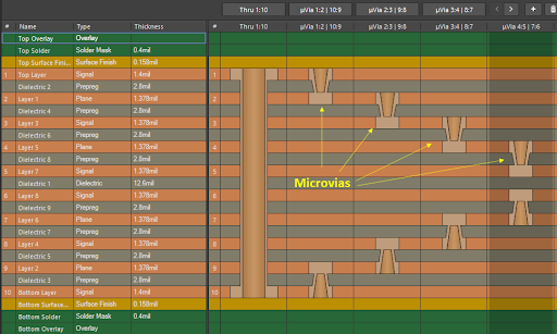
This ability to specifically call out a via as a microvia is useful once you go to set up design rules and create via templates. To set up your design rules for routing with vias, you can define a design rule as only applying to microvias. This lets you set specific limits on clearances, via pad size, and hole diameter. In Altium Designer, you’ll want to use the “IsMicroVia” portion of the custom query below to ensure the design rule applies to microvias on a specific Net Class.
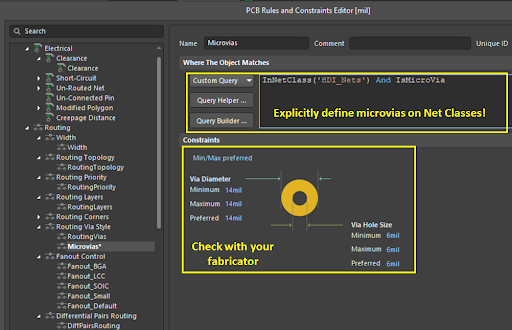
Note that the via width and pad size defined here were taken from fabricator capabilities for an earlier project. You should consult with your fabricator regarding their capabilities before you start setting up design rules. Your trace width then needs to be set in your design rules to ensure your trace impedance is controlled to the desired value. In other cases, where impedance control is not needed, you may still want to limit trace width in an HDI board to keep routing density high.
Trace Width
You can determine the required trace width in a number of ways. First, for impedance controlled routing, you’ll need one of the following tools:
- A pen and paper to calculate the required trace size (the hard way)
- An online calculator (the quick way)
- A field solver integrated in your design and layout tools (the most accurate way)
I’ve discussed the drawbacks of using an online calculator for trace impedance calculations in a different article, and the same points apply when sizing traces for an HDI PCB layout.
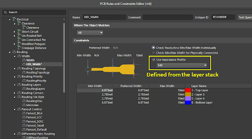
To set up the trace width, you can define it as a constraint in your design rules editor, just like you would with via sizes. If you’re not worried about impedance control, you can set whatever width you like. Otherwise, you need to determine an impedance profile for your PCB stackup and enter this specific width as a design rule.
There is a careful balancing act you’ll need to play as the trace width can’t be too large for your via landing pad size. If the impedance controlled trace width is too large, you should decrease the laminate thickness as this will force the trace width to decrease, or you can increase the landing pad size. As long as the landing pad size exceeds the value listed in the IPC standards, you’ll be fine from a reliability standpoint.
Once you’ve determined the width you need for impedance control, just set this value as a design rule. In Altium Designer, you can use the integrated field solver to define an impedance profile, which can then be used to enforce a required width in your design rules.
Clearances
Once you’ve done the two critical tasks shown above, you need to determine the appropriate trace clearance. Unfortunately, you shouldn’t default to a 3W or 3H rule of thumb for spacing between traces as these rules are incorrectly applied to advanced boards with very high speed signals. Instead, it’s better to run a crosstalk simulation for a proposed trace width and check whether this will produce excessive crosstalk.
Import From Schematic and Share on Altium 365
Once you’ve finished setting up your design rules, routing constraints, PCB layer stack, and via styles, you’re ready to capture your schematics as an initial layout. If you’re working with a remote team and you need to collaborate on an HDI PCB layout, you can share your new layout in your Altium 365 Workspace. Your collaborators will be able to edit the layout within Altium Designer, and your team can collaborate with your fabricator to ensure your board can be produced at scale. You’ll also have access to a complete set of version control features, user access management tools, and component repository.
The design rules and constraints shown here can be easily applied to an HDI PCB layout thanks to the rules-driven design engine in Altium Designer®. Once you’re ready to start your PCB layout, you can use Altium Designer and the Altium 365® to create a productive workflow for your remote PCB design team.
We have only scratched the surface of what is possible to do with Altium Designer on Altium 365. You can check the product page for a more in-depth feature description or one of the On-Demand Webinars.