Complete Guide to DIY SMT Assembly In Your Office
I want to share a little secret with you in this article: Assembling SMT prototypes boards is not only easy, but it requires very little equipment. Using just a stencil, I can easily hand prototype down to 0.3 mm pitch ICs, and 0201 (imperial) sized passive components. Tiny wafer-scale components can definitely be a challenge, but the majority of prototypes that are regularly produced can be hand-assembled in a couple of hours with production quality results, including double-sided boards. If you’re currently hand assembling boards with a soldering station, you need to stop this immediately and start using a stencil instead!
Most low-cost printed circuit board manufacturers also offer an unframed stencil service for around $5 to $25, depending on your board’s size. The stencils and boards I’m using in this article are purchased from JLCPCB; however, some other suppliers’ have stencils that are comparable. If you have rush ordered your boards from a local board supplier, there are companies on most continents that sell low-cost, unframed Kapton, acetate, or stainless steel stencils. Alternatively, if you have a CO2 laser cutter, you can easily make a stencil from an acetate photocopier transparency sheet. However, that’s getting a bit too far away from this article’s scope.
Using a stencil makes board assembly highly forgiving, much faster, and a lot easier than soldering each component. A stencil allows you to assemble using components that are impossible to hand solder, such as BGA components or leadless packages with their exposed pad under their center that you just cannot reach with a soldering iron. Using simple tools and requiring a lot less effort than individually soldering each component, you can produce a board that looks like it came off a pick and place line in less time than it takes you to have a quotation for your pick and place job.
Tools and Supplies
No matter how well (or poorly) equipped your electronics lab is, assembling your own boards requires very little equipment to achieve fantastic quality results. You probably already have the supplies you need, and if not, you can obtain them very cheaply. This process is equally suitable for students starting out and for professional engineers rapidly prototyping at multinational companies.
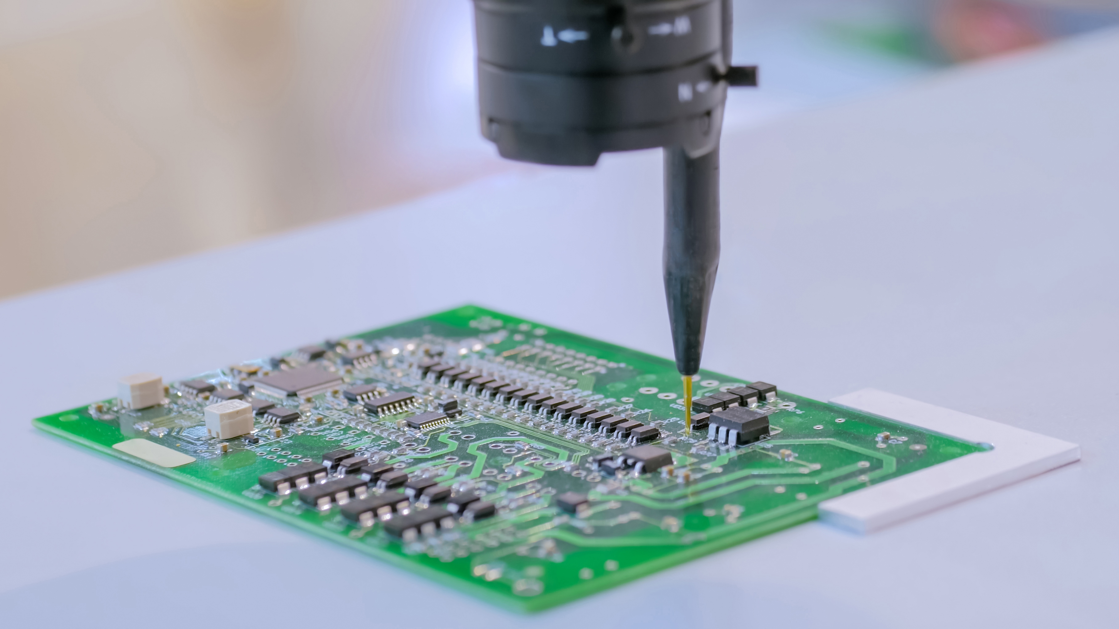
In addition to tools and supplies, you should have a very well-lit workspace. Working with small components can quickly lead to eye fatigue if you do not use high-quality lighting. I have two LED light panels designed for videography work mounted over my workbench, and a good quality magnifying lamp can also be extremely useful. If you’re not working with small enough components to need to use the magnification facility, taking the lens out of the lamp can let you see better as your breath won’t fog up the lens!

To get started, you’ll need some solder paste – and Loctite/Henkel GC 10 in T4 mesh is an excellent paste for handwork. It can be stored at room temperature, and it gives you hours to finish your hand assembly while still allowing you to reflow your board successfully. This is a lead-free SAC305 solder, which offers superb results.
For handling the solder paste and cleaning up afterward, you will want some nitrile gloves. This stage can get a little messy, and it’s much easier to throw away a pair of gloves than try to clean sticky solder paste off yourself.
To clean up the solder paste, you will need some Isopropanol, also known as Rubbing Alcohol or Isopropyl Alcohol. This makes effortless work of cleaning your stencil. You’ll also want some paper towels to wipe things with afterward.
To apply the paste, you need a squeegee of some sort. I typically use a credit card-sized piece of plastic, like an unwanted store membership card. Avoid using a metal device like a scraper or spatula as these can cause damage. The squeegee you use should be softer than the stencil material, if possible. That way, you’re letting your valuable stencil damage your easily replaceable squeegee rather than the other way around.
To mount your board precisely, you will need something to hold it in place with the same thickness as the board. In this article, I’m using some 3D printed surrounds; however, you can use laser cut 1/16 inch acrylic or use some spare/scrap unpopulated PCB. The advantage of using my 3D printed surrounds is that I have added a lip around the outside, which allows the masking tape I’m using to mount the surrounds to be lower than the top of the surround. The surround not only holds the board in place precisely, but it also provides support for the stencil so it cannot bend or lift away from the circuit board as you work.
In this article, I will use a laser-cut acrylic board for mounting the circuit board, but this is primarily for my convenience. In the past, I’ve almost always simply taped everything down to my desk! Any masking tape will do; however, I’m using a nice and thin 3M tape that is 1.5 inches wide - it’s wider than typical masking tape, making life a lot easier.
Once you have applied the paste to your board, you’ll need some good quality tweezers to place the components. I use Swanstrom 7-SAH tweezers, which have a large padded grip that makes them comfortable to use for extended periods. They are made from high-quality stainless steel, which doesn’t easily bend when using them for peeling any cover tape off components.
After the components are placed on the board, you will need to heat the board to melt the solder. You do not need to use anything fancy for this job - a converted pizza/toaster oven or an electric skillet will work perfectly. Personally, I typically use a cheap 858D hot air rework station, which means I need to move across the board, heating it up as I go to melt the solder. As a result, it takes a little longer to reflow each board; however, it’s an inexpensive tool that I already have. I also have a silicone cooking mat to protect my ESD mat and workbench from the heat. If your board has some very large ground pours, thick copper, or multiple ground layers, then a low-cost electric skillet works extremely well as a preheater plate. The hot air rework tool can then be used to take the solder up to its peak reflow temperature.
Framing the PCB
I start by framing up the PCB on my work surface. We want the surround to be tight-fitting on all four sides to fully constrain the board that you will be applying the paste to. It should have support on all sides, which should be the same thickness as the board itself, so it will support the stencil once it’s placed on top.

I use masking tape to hold the surrounds down, as the tape is thin and easy to remove once I’m done.
Once you have the surround in place, you will need to tape your stencil in place. I build a hinge at the back of the stencil using tape, which will hold the stencil in precise alignment with the pads. Alignment is critically vital if you have any extremely small or fine pitch components. An 0201 pad can very easily be missed entirely if the stencil alignment is even slightly off. Thankfully, it’s straightforward to line up the stencil; just keep moving it bit by bit until every aperture on the stencil shows a bright shiny metal, and there is no solder mask visible.
The back of your stencil will also need some supporting material so that the back of the stencil where it is hinged is at precisely the same height as the PCB that you’re applying the paste to. Once your stencil is perfectly aligned, run a strip of masking tape across the back to hold it in place. This will allow you to lift the stencil off the board without smudging your freshly printed paste.

Applying the Paste
If you’ve ever done screen printing, you’re probably already an expert when it comes to applying solder paste - it’s exactly the same process. If you haven’t, never fear, it’s very easy!
First, collect a good-sized blob of solder paste on your squeegee; I use a credit card-sized piece of plastic, using the narrow side so that the pressure I apply is consistent across the whole width of the squeegee. The paste you collect using your squeegee should cover the full width relatively evenly.
With one hand, hold the stencil down firmly onto the surround so it sits perfectly flat and correctly positioned on the board. Do not lift or move this hand until you have completely finished!
Start off with your squeegee located over the stencil aperture on the opposite side of the stencil from yourself. The first bit of paste should be applied to an uncut part of the stencil over the surround and not onto a stencil opening. With firm pressure, draw the squeegee towards yourself; the excess solder you have on your squeegee should be pressed into the stencil. Having a good smear of solder paste left after you are done is perfectly acceptable. Having stencil openings that are not entirely filled is not good enough. If this occurs, try again, making sure that the stencil does not move or lift at all.
When the stencil openings have all been correctly filled, make a final light cleanup pass over the stencil with your squeegee held vertically. Here, you’re just looking to clean up the excess solder paste. This should leave all your stencil openings filled to the brim with solder paste. If you press too hard during this step, you may actually pull some of the solder paste out of the aperture and leave yourself short of paste on some pads. It’s generally better to have slightly too much solder paste than too little.

Once the stencil looks relatively clean (it should not take more than one cleanup pass to achieve this), put your dirty squeegee aside on a piece of paper towel. You should still have one hand holding pressure on the stencil at this point; only know can you get ready to move it. Lift the front of the stencil straight up while keeping pressure on the rest of the stencil. Release the stencil slowly as you continue to lift it as straight as possible - you do not want the stencil to move laterally as this will smear your solder paste.
Once the stencil has been completely lifted from the board, you can inspect the solder paste. It should be sharply defined with flat tops on each pad of paste. If you have smeared the paste (remember to check the finest pitch components thoroughly), you will need to start again. You’ll have to completely wipe the solder paste from the board using a paper towel soaked in isopropanol and go back to the beginning of the process. Similarly, if it looks like you have well-defined pads, but there are smears of solder between them, your stencil lifted while you were applying the paste. Again, you’ll need to thoroughly clean the board and try again.
Once you have mastered the technique for applying the paste and lifting the stencil, your success rate will become extremely high, and it will be thankfully rare that you will need to clean the paste off your board.

Before moving on to populate your board, place some paper towel where your circuit board was, and then clean your stencil with an isopropanol soaked paper towel. It’s much easier to clean up as you go along rather than forget to clean your stencil and later find it covered with rock hard solder paste that’s nearly impossible to clean off!
Populating the PCB
If you’ve ever hand-soldered many components to a circuit board, you are going to love this next step. It is so easy in comparison.
We now just need to run through our bill of materials and place the parts down on the board. Using curved tweezers makes this much easier, as you don’t need to plan the order of your placement quite so well - the tweezers let you reach over other components reasonably easily.
I suggest looking at a 3D view of your board using Altium before you start to determine which components are likely to get in the way of your hand and plan to place them last. If you have high-density areas of components on your board, place your most critical and challenging to access components in those areas first. Components like resistors and capacitors can be placed last in those areas as their alignment is less critical. If you have trouble accessing their pads, you can simply drop them into the right spot as best as possible and then nudge them into the correct place.
Place the largest components such as inductors, aluminum capacitors, and surface mount connectors last - these are the most likely to get in your way as you place other components.
Your placement of components is important but not highly critical. Generally, as long as the component’s leads are touching the solder paste, the alignment is good enough. This makes leadless components easier to fit than you might otherwise expect. As long as the component is pretty much correctly over the footprint, it will sort itself out once the solder melts. Once each component is in place, gently press it down into the paste to ensure you have good contact with the flux. This also makes it harder to accidentally bump components off their pads as you work around them. When you come to heat the board using hot air, having the components making good contact with the tacky flux will also reduce the likelihood of accidentally blowing them off your board if you get a little too close with the hot air!

If you have shaky hands or tremors, it can be a real challenge to place the smallest components. If I’m having trouble getting a part perfectly aligned, I use my left hand to brace the tweezers while holding them in my right hand. This two-hand operation helps reduce any shaking and allows me much finer motor control. This really helps with placing the finest pitch and smallest components.

Dinner Time
With all the components correctly placed on your board, it’s time for the really fun part - cooking your board.
As I mentioned earlier, I’m just using a very cheap hot air rework gun for the purposes of this article to show how inexpensive and easy this process can be. With my board sitting on my silicone cooking mat, I start heating the board with the rework station set to 350 oC and its maximum airflow setting.
Start off by heating with the heat gun a reasonable distance away from the board, moving across all areas of the board. To start with, you are just trying to warm the whole board up, getting heat into the larger copper areas and pours. If you have large inductors or transformers on your board, you want to get those warmed up as well, as they will need a lot of heat pumped into them. As you heat the board, you’ll see the solder paste turn glossy as the flux starts to become more liquid. Your goal at this point is to heat the board, but not to heat it so much the flux gets driven off.
Once all your paste is looking nice and glossy, it’s time to bring the heat gun in closer, but keeping it about 1.5 to 2 inches (35 to 50 mm) away. Don’t get too close; the heat gun is set much hotter than it needs to be and could damage your components or the PCB. You might also blow some small parts off their pads before the solder has melted! Start working the gun in small circles over your first set of components. You’re trying to bring the components and their pads up to the melting point of the solder and heating any large copper pours so the pins connected to these areas will reflow at the same time. I never use thermal relief on any of my boards and have absolutely no problem with boards reflowing evenly using this low tech approach.

I love watching the solder paste melt and become shiny, with the components centering themselves on their footprints. Once the solder on every pad in the area has completely melted, keep heating the area for an extra 2 to 3 seconds before slowly moving the heat away to other nearby areas. You don’t want to move too fast, or your solder will cool too quickly. Conversely, you don’t want the heat to dwell too long, or the solder will oxidize too much.

If you’re unsure if the solder has melted under a leadless component, use your tweezers to carefully nudge it a tiny bit. A component resting on molten solder will float off to the side and then bounce back under surface tension if the solder has melted. A component that is on unmelted paste won’t nudge aside as easily and won’t recenter when you move your tweezers away.
If a component wasn’t lined up well enough and jumped to a weird angle during the reflow, you can just float it back to the point where it snaps into the correct alignment using your tweezers. While the solder is molten, you have a lot of freedom to move components around by poking them with your tweezers. The molten solder’s surface tension will make components sit directly over their footprint when you have them in the right alignment and generally ensure you don’t get any bridged pins. If you do get visibly bridged pins, you can fix this later with some flux and soldering iron, or you can lift the component off the board while the solder is molten then drop it back into place. Bridged pins are usually a sign that you had too much solder paste on the board.
Again, try not to keep heat applied to an area for too long when you fix problems. This can cause the solder to oxidize too much, which can give you a poor quality joint. If you do find an issue that you don’t think you can fix in a few seconds and you don’t think you can fix it with a soldering station later – just leave it for now. Once you are finished reflowing the board, you can apply gel flux to the components in the area you will be heating, mask off the other others nearby with Kapton tape, and then reflow that area again. The gel flux will give you time to fix your mistakes and clean any oxides off the solder as you go. Be warned; gel flux can be very messy to work with and will need a lot of cleaning afterward.
Final Work
For this particular board, I forgot to order one line item, which was a capacitor. Luckily, I had a capacitor with the same value and rating leftover from another project that I could use. The only problem was the package was much smaller. For this board, I just needed to solder this capacitor on afterward, but it’s much easier to solder components onto the board while it’s still warm from your reflow activity. Always take advantage of the residual heat if you need to add any through-hole parts or last-minute fixes.

Double-Sided Boards
To solder a double-sided board, you just follow exactly the same procedure for the opposite side. You’ll need to either build up the support for your board to make room for the components on the bottom side or simply cut a pocket out of a base as I did with my acrylic board for this PCB. Try to solder the side with the least critical and smallest components first so you won’t generally have any problems with components falling off as the molten solder’s surface tension will hold them on. It’s easier to leave your most complex side for the second heat.
If you are particularly worried about the bottom side’s components becoming detached or misaligned during the second heat, use a Tin Bismuth solder paste on the second side. Its melting point is much lower than a SAC305 paste, which means that the solder on your bottom side won’t even notice the heat by the time you have the SnBi paste successfully reflowed.
Have Fun!
Hopefully, this article has shown that reflowing a board with primitive low-cost lab tools is relatively trivial and gives you high-quality results. Many people who have not tried using a stencil themselves express amazement that I can work with 0201 components or very fine pitch leadless components by hand. But the truth is anyone can do it. With a simple stencil and quality paste, you’ll be amazed at what you can achieve. Leave the soldering station switched off when you’re populating boards; there are more efficient ways to do this than soldering each component individually.
The design tools in Altium Designer® contain everything you need to keep up with new technology. Talk to us today and find out how we can enhance your next PCB Design.