Best Design Practices for Double-Sided PCB Soldering with SMD Parts
DFM guidelines tend to focus on fabrication, but PCB assembly should also be considered in the design to ensure a board can be fabricated without defects. Double-sided PCBs, where components are placed on both sides, carry some important assembly guidelines to prevent warpage and low solder strength. Like other manufacturing defects, there are some steps a designer can take to ensure their double-sided PCBA will have high yield. Here’s what you can do to ensure high yield after double-sided PCB soldering.
The Double-Sided PCB Soldering Process
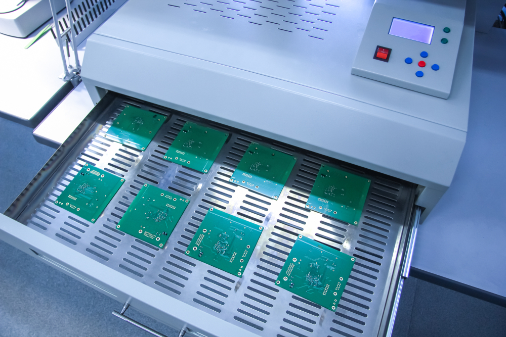
For double-sided PCBs with SMD components, the board will need to go through sequential reflow soldering unless you opt for hand assembly. Reflow soldering will be used on high volume runs/low-cost prototyping runs, so designers should plan for reflow soldering during assembly. In the double-sided PCB soldering process, components are placed and soldered on each side of the board individually. The trick here is to solder at just the right temperature and time as the components on the first side will be going through reflow soldering twice.
During this process, some defects can occur on double-sided PCBs. The principal defect is warpage, while the secondary defect is a weak or failed solder joint. Applying the process to a double-sided board does not necessarily require special equipment, but running the process twice puts the PCBA at risk of experiencing defects. There are some basic steps designers can take with double-sided boards to prevent these defects:
Opt for a Thicker Substrate with Symmetric Stackup
Thinner boards will be more susceptible to warpage during reflow soldering; if it’s less than the standard PCB thickness and you put yourself at risk of warpage. The stackup should be symmetric as well so that thermo-mechanical stress is more evenly distributed throughout the board. It’s also advisable to use prepreg and core laminates with similar resin content and glass weave style as their CTE values with be very similar.
Opt for a Higher Tg Substrate
Using a substrate with higher glass transition temperature Tg will help prevent warping during sequential reflow soldering simply because the board will experience less expansion than a low Tg substrate. The Tg value for standard FR4 substrates is about 130 °C for substrates classified as “low Tg,” or greater than about 170 °C for substrates classified as “high Tg.” This is below the typical peak reflow temperature for Pb-free (Sn/Ag) solder, which can reach 240-250 °C. Therefore, opt for a higher Tg substrate to help prevent warpage during double-sided PCB soldering.
Double-Sided BGA Soldering
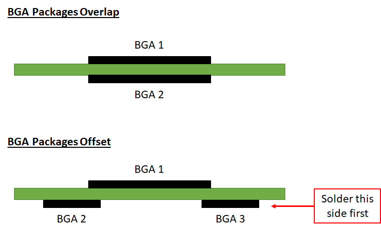
What about soldering BGAs on both sides of the board? Multiple large BGA packages are not so common, but micro BGA packages are becoming more common and are a popular option for small components. Just like other SMD components, you can place them on both sides of a board for a double-sided PCB reflow soldering process. The question is then, how can you design the board to ensure the highest possible yield?
The typical method is to use a mirror image, where identical packages are placed directly behind each other (think of a RAM stick). In the case where packages are mismatched, the component arrangement will also be mismatched. The preferred order would be to put the smaller, lighter BGA packages, as well as smaller SMD components, on one side of the board and solder these first. Then place the larger BGA on the opposite side and send it through reflow second. This way, the lighter parts will have lower chance of desoldering or empty/false welding during the second pass. The ideal case is shown below, where multiple packages are mounted on each side of the board.
Expect Heavier Parts to be Soldered by Hand
Heavier parts, such as a transformer or bulky connector, should be hand soldered or processed with selective soldering as it’s difficult to counterbalance their weight across the board. In general, it’s difficult to distribute parts so that weight is balanced across a single board surface, so don’t expect to start perfectly balancing heavy parts on every double-sided PCB. Instead of putting heavier parts through the reflow process, have these done by hand to prevent warpage and ensure high yield.
Reflow Profile on Side 1 vs. Side 2
Next is the question of the reflow profile on each side. How should the reflow profiles be constructed? Should they be the same on both sides of the board? There isn’t a firm answer to this question as it depends on the components being soldered and whether there is a surface plating on exposed conductors. The surface plating is particularly important as intermetallics can form during soldering:
- Exposed copper: Tin in the solder alloy can form Cu-Sn intermetallics, which slowly grow and eventually become brittle during soldering. Reduce the overall time at higher temperatures by getting up to the peak reflow temperature quickly.
- Electroplated nickel and electroless nickel: The intermetallic alloy Ni3Sn4 most commonly forms during soldering with tin-based solders, although the formation rate is much lower than Cu-Sn intermetallics.
- ENIG, ENEPIG, OSP, and immersion Ag: Cu-Sn/Ag intermetallics can form on these platings at the interface, rather than diffusing into the bulk. Interestingly, the Ni layer inside of ENIG and ENEPIG has a toughening effect on some intermetallics, which prevents crack formation.
Without going much further into the chemistry, the important takeaway here is that the reflow profile for a double-sided PCB should be designed to accommodate various PCB surface platings for double-sided boards. There are some interesting studies that look at the formation rate of different intermetallics, and these can provide some guidance for comparing reference reflow profiles. Here are two great references where you can learn more:
- Shen, et al. "Packaging reliability effect of ENIG and ENEPIG surface finishes in board level thermal test under long-term aging and cycling." Materials 10, no. 5 (2017): 451.
- Guoyuan, et al. "Effects of surface finishes on the intermetallic growth and micro-structure evolution of the Sn3. 5Ag0. 7Cu lead-free solder joints." In 2009 International Conference on Electronic Packaging Technology & High Density Packaging, pp. 807-811. IEEE, 2009.
If you’re designing a new product that will require double-sided PCB soldering, use the complete set of PCB design and layout tools in Altium Designer® to create your board and prepare for manufacturing. The Layer Stackup Manager and upgraded Design Rules Editor help you create a high-quality board that complies with DFM/DFA standards for double-sided PCBs.
When you’ve finished your design, and you want to share your project, the Altium 365™ platform makes it easy to collaborate with other designers. We have only scratched the surface of what is possible to do with Altium Designer on Altium 365. You can check the product page for a more in-depth feature description or one of the On-Demand Webinars.
