What is ESD and How Does it Affect My PCB Design?

In some environments, accumulation of static charge means that the shocks are much bigger when they occur. As kids, we used to scoot across the carpet in our socks and try to shock each other. As a designer who needs to handle circuit boards, this is not a great idea as it will damage certain components in your PCB.
While I’m still surprised when I receive a static shock, I’m not damaged. This is not true for electronics, which can be destroyed by voltages so small that you’d never feel them. As a result, it’s important to plan for mitigation and ESD protection in your PCB designs.
What is Electrostatic Discharge (ESD)?
Electrostatic discharge (ESD) occurs when two objects with different charges get close enough, or charged enough, to break down (ionize) the dielectric between them. For consumer products, ESD and dielectric breakdown in air usually occurs when the electric field between two points is greater than 40 kV/cm. Things like air pressure, temperature, and humidity will affect this electric field strength. For example, high humidity in some environments can cause the air to be more conductive, which will dissipate some charge and increase the voltage required to ESD.
One common misconception is that a specific voltage is needed to cause ESD. This is not exactly correct; the voltage required to produce ESD is dependent on the voltage between two points and the distance between those points. This is why, in PCBs, we have a limits on the clearance between conductors (creepage and clearance) as specified in the IPC-2221 standards.
Lightning is the form of electrostatic discharge that people are usually most familiar with when clouds and the earth form a giant capacitor. Less dramatic is when you shake a fleece or wool blanket at night and see the little sparks jump. No matter how it's caused, ESD produces some undesired effects in a PCB.
How Does ESD Affect a PCB?
Any printed circuit board may be subject to an ESD if it’s touched or comes close enough to people, packaging, cables, or any other object that might produce a large potential difference. When this voltage difference is large enough, there will be a conductive path for current, creating a massive current pulse. As the current pulse develops, high heat is dissipated within the components and the conductors on the PCB itself. At extreme field strengths and developed currents, the PCB can be damaged and components can be destroyed.
This heat dissipation is basically IR drop, where the natural DC resistance of elements in the PCB create a voltage drop and reach high temperature. ESD can occur in some common locations on a PCB, so ESD protection in a PCB should be focused in some particular areas.
ESD in Integrated Circuits
The ESD pulse can cause the path followed by current to flow through the die on an integrated circuit, creating high heat that destroys a component. An example on an integrated circuit package and traces on the semiconductor die are shown below.
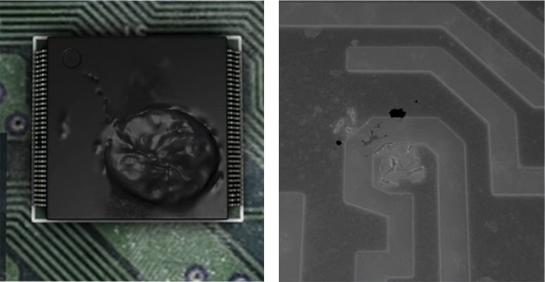
In particular, many modern chipsets are made using such small lithography features that they have little or no tolerance for a high voltage drop, even for DC values slightly above their operating voltage (3.3V or less). The result of an ESD event directly reaching one of these electronic components is usually disastrous, completely ruining the IC and producing the kind of damage shown in the right panel above.
ESD in Connectors
Connectors themselves are not sources of ESD, but any static charge that might build up on them can cause an ESD event. Every time someone plugs something in pulls a cable out, or pushes a button, they’re introducing static risk to the device. There is the potential for floating pins to create an ESD event due to static charge handing on the floating conductor. Finally, there is the potential that an ESD event occurs as the connector is plugged into its receptacle, creating a visible spark.
The simple solution for dealing with floating pins is to ground them. Shielded connectors should also have grounded shielding connected to the chassis and, eventually, the earth ground connection. Both steps will dissipate any discharge current back to ground. This should be a direct low-reactance connection that immediately to the chassis; don't provide this connection through a capacitor, and don't route an ESD current through the PCB to ground.
Nearly every element of your PCB design (traces, routing, layers, electronic component placement, and spacing) can affect the PCB ESD protection on your board. That means you need to consider ESD protection circuits early in your design process; otherwise, you’re likely to require a major Circuit Board redesign to fix routing and electronic component placement issues.
Implementing ESD Protection on a PCB
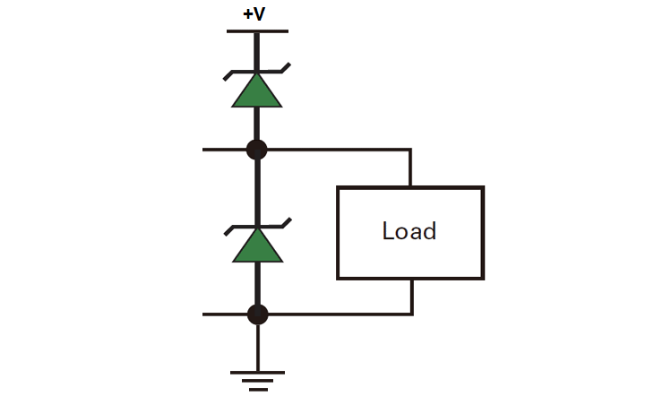
The goal in implementing ESD protection on a PCB is to prevent an ESD current from flowing into your circuits and instead divert it into ground through a low-reactance connection. Just as is the case for a connector, this ground should be off the PCB. A standard circuit used on the I/OS of some ICs placed near potential ESD sources (like a connector) is a Zener diode (transient voltage suppressor). This small circuit uses 4 Zener diodes that are reverse biased during an ESD event, creating a shunt connection for the high-voltage/current and protecting the rest of the PCB. This should be placed very close to the source so that current can be immediately shunted to ground.
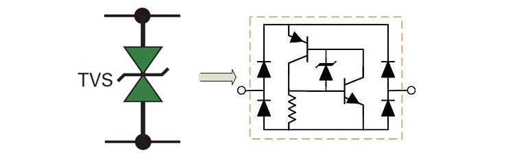
Other ESD protection devices include gas discharge tubes, TVS diodes, and simple varistors. Note that a TVS diode, which is the other common method for implementing ESD protection on important interfaces, is not a simple diode, as shown in the equivalent circuit below.
ESD protection for USB, Ethernet, I2C, RS-485, RS-232, and other digital interfaces will generally use a TVS diode between a connector and the IC containing that interface. This is in addition to shielding any metal connector shrouds and unused pins. Your component datasheets will often have some guidelines you should follow to ensure ESD protection. Some companies will also list specific ESD ratings in the datasheets, which might comply with specific industry standards (e.g., automotive or telecom standards), and you might opt for these components when you're designing equipment that might be prone to ESD exposure.
With the best PCB design tools in Altium Designer®, you can implement ESD protection in your PCB, enclosure, and other areas of your electronics to ensure they stay protected. When you’ve finished your design, and you want to release files to your manufacturer, the Altium 365™ platform makes it easy to collaborate and share your projects. We have only scratched the surface of what is possible to do with Altium Designer on Altium 365. You can check the product page for a more in-depth feature description or one of the On-Demand Webinars.
