USB Charger Project in Altium Designer: Part 1

When I’m in my office, I keep my pluggable USB charger around, otherwise the battery on my phone is likely to run out. If you want to build your own USB charger, you can create your own USB charger board with the powerful schematic design and layout tools in Altium Designer. Here, I’ll present the overall design process for a portable USB charger. The charger requires 12 V of power and charges two external devices through two USB ports. We’ll take a look at the process for creating the schematic first, and the layout process will be shown in an upcoming article.
Getting Started with the Schematic
This board is electrically simple enough that it can be routed on a 2-layer or 4-layer standard thickness board (1.57 mm), but it still requires some important considerations in the schematic and routing portions of the design. This design will feature 2 USB charging ports with LEDs as indicator lights. To get started with the schematic, you’ll need to start with a parts list and think about whether you’ll have to arrange parts in a single schematic or in multiple schematics. Here, I’m going to show everything in a single schematic as the part count is not terribly large. In this project I have the following list of parts:
- 2 standard USB A connectors
- LM73606 buck converter: used to step-down the 12 V input
- 2 LEDs: used as indicator lights
- 1 iron-core inductor (used in the buck converter feedback loop), 13 resistors, 19 capacitors
- 2 TPS2549 USB switches (1 for each connector)
All components are surface-mount components. Although not components per se, there are three Socket connectors that will appear in the schematic. This is essentially a pad that is used to connect to the power supply (see the 12V, GND, and DIM sockets). You can find the Socket component in the Miscellaneous Connectors.IntLib library file. The rest of the required components can be accessed from the Manufacturer Part Search panel or from an existing library.
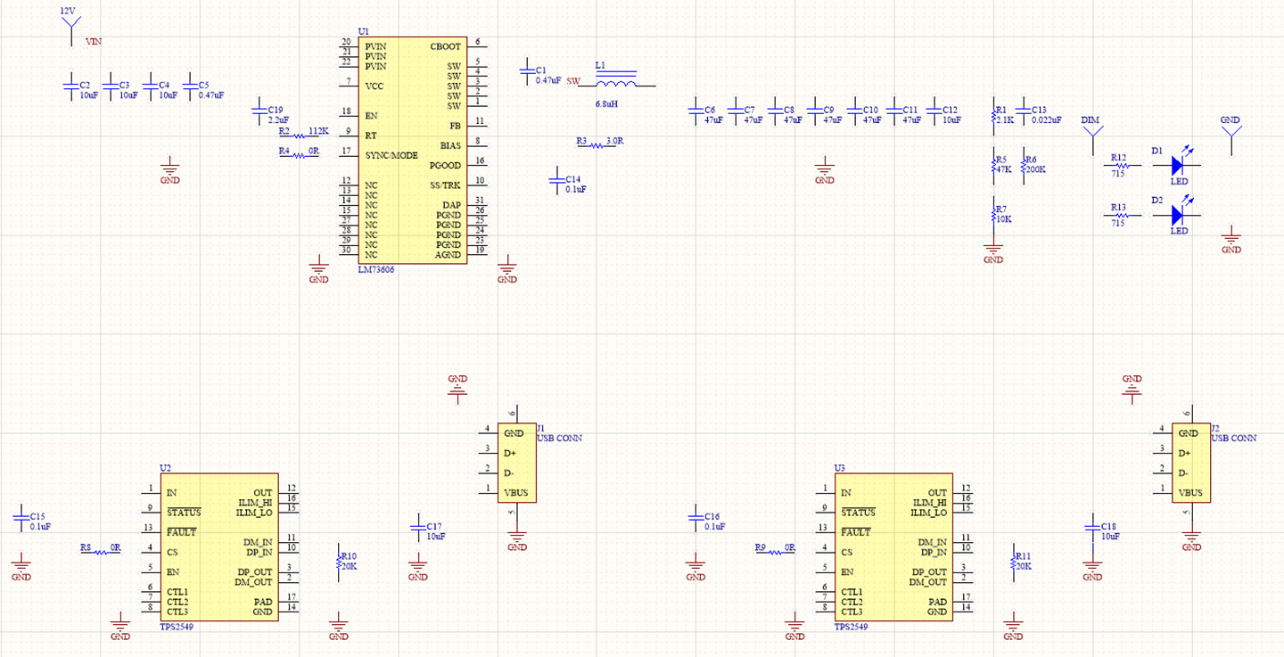
To get started, I’ve placed everything in a single schematic as the part count is not so high as to warrant hierarchical schematics. The image below shows the initial schematic without any connections between components. I’ve laid out the schematic in this way just to develop an initial floor plan as it is easier to move around unconnected components.

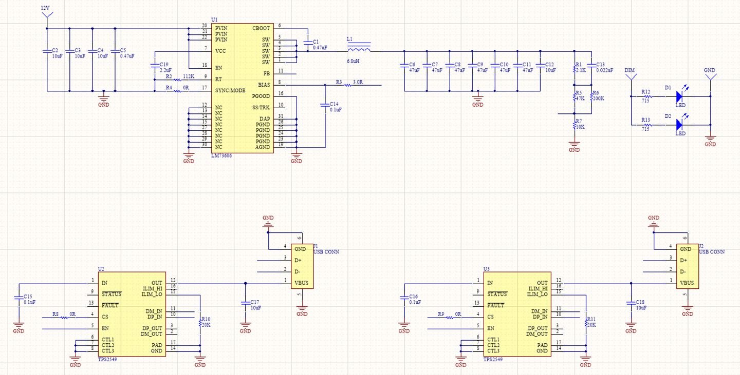
The bank of capacitors in the upper left are intended for decoupling/bypassing on the input power. The second bank of capacitors in the upper middle portion of the schematic are part of the buck converter feedback loop. The output from the LM73606 uses two decoupling capacitors to ensure stable power reaches the TPS2549 USB switches. These decoupling capacitors are C14, C15, and C16. The LM73606 is a synchronous DC-DC converter, so the feedback line is wired up for synchronous operation by following the guidelines in the LM73606 datasheet (see page 12).
Note also that the inductor in the feedback line is rather large as this is intended to reduce ripple on the output from the buck converter circuit (see page 13 of the LM73606 datasheet). If you want to use a larger switching frequency, you could then use a smaller inductor while still meeting your ripple requirements.
Once you’re satisfied with the initial arrangement of components, you can start wiring everything together. My wired schematic is shown below:

The next step is to assign some net labels in different portions of the schematic. This makes it easy to track where different connections are going throughout the schematic and to see different nets in the schematic and PCB layout editor windows.
Compiling Your Schematic
Once you’ve wired up an initial schematic and assigned some net labels, you’ll need to compile the schematic. In Altium Designer 20, this happens automatically in the background. However, if you’re still using Altium Designer 19, you’ll want to right-click on the project file in the Projects Panel and click Compile. At this point, I get a window showing warnings about unconnected pins in ICs. The astute designer should notice there are some unconnected outputs from these components.
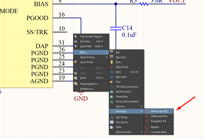
As we can skip those messages, we can update the schematic library or add No ERC mark on those pins. I’ll assign a Generic No ERC on these floating pins. An example for the LM73606 is shown in the image below the (SS/TRK) pin. Click the right mouse button and select “Generic No ERC” or press ‘P’+’V’+’N’ on the keyboard. Although these outputs can be left floating, it is helpful to just suppress these warnings as they can get annoying after awhile.

One important point to note is that pins DM_IN and DP_IN on each TPS2549 are a differential pair that connect to the two center pins of the USB A connector. Be sure to assign a Differential Pair Directive to each of these pins. The net label with the positive end must be named using “_P” at the end of the net label, and the negative end must be named using “_N”. Assigning these net labels in the schematic helps prevent any confusion and allows the differential pair to be easily simulated in your layout.
At this point, the schematic is basically finished. If you like, you can bring the capacitor banks and feedback section into simulations to examine their immunity to noise and tolerance to heat. This can help you assess which steps will be required to ensure proper operation in your layout.
I’ll create the layout in Part 2 of this project. If you’re looking to create a new schematic for your own USB charger project, you should try using the full suite of CAD features in Altium Designer®. This powerful PCB design platform gives you access to all the design tools you need for this project and many others in a single application. You’ll also have access to a full set of pre-layout simulation features, signal integrity simulation features, and production planning tools.
Now you can download a free trial of Altium Designer and learn more about the industry’s best layout, simulation, and production planning tools. Talk to an Altium expert today to learn more.
