Understanding Ground Planes in Your Two-Layer PCB
Back when I was a young and hungry grad student, my first PCB ground plane design was used to collect analog signals from several sensors. When looking at a voltage graph of my measurements, the noise level was horrible and completely masked the signal I was trying to measure. I soon realized that I had completely bungled my ground plane connections, and ground loops were ruining my signals.
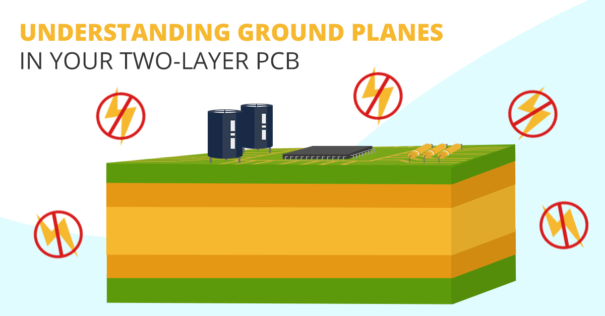
Placing your ground plane and routing to ground are two of the most important design guidelines in PCBs with two or more layers. Doing this correctly can help reduce susceptibility to EMI, suppress crosstalk, and prevent ground loops. These noise sources degrade signal integrity, and proper circuit board ground plane design techniques will ensure that your device shows maximum performance.
Does My Two-Layer PCB Need a Ground Plane?
If you're new to PCB design, your first PCB will likely to be a two-layer board as they are relatively simple to work with from a layout and signal integrity perspective. You'll have limited real estate as you won't be routing signals through an internal signal layer. This is the first point to consider when determining whether to include a ground plane and where to place it on the board. Most PCB designers will swear by using a ground plane, and this is certainly the best choice when working with high speed/high frequency signals. From an EMC perspective, separating a ground plane from the signal layer of the PCB will provide some level of protection from radiated EMI from external sources.
Using a 2 layer PCB ground plane is also preferable to just routing ground traces. Routing a return trace adjacent to a signal trace is one strategy to minimize EMI susceptibility in multi-board designs when high speed/high frequency signals are routed between boards through a cable. Placing a ground return as close as possible to a signal line allows the return signal to closely follow the trace, which minimizes loop inductance and EMI susceptibility.
Nearly every board that includes multiple components will simply not have enough room for routing return traces alongside all signal traces. Placing a ground plane on the bottom layer of a two-layer PCB provides the same effect; placing the ground plane below signal traces also reduces the loop area seen by signals. Ideally, signal traces should be placed as close as possible to the ground plane to suppress crosstalk between neighboring traces, which might require using a thinner board.
Placing a ground plane below the relevant components and signal traces also allows you to route ground returns directly from a component to the ground plane through a via. The return signal will then follow the path of least impedance back to the power supply return. This also allows you to easily place bypass/decoupling capacitors between power connections on critical components and the ground plane, which allows any high frequency fluctuations in the power connection (e.g., conducted EMI from a switched power supply) from reaching the relevant components.
Prevent EMI with proper routing and grounding techniques
Gridding with Ground Plane Sections
Rather than place a continuous ground plane across the entire bottom layer, one technique that can be used in a two-layer PCB is gridding. Power and ground traces are routed in a differential manner, mimicking a pair of power lines. Every ground trace can be expanded to fill up as much of the empty PCB space as possible, and all the remaining empty space can be filled with ground pour. This technique will give your 2 layer board the same level of noise reduction as a four-layer PBC stackup.
One other solution is to use two perpendicular grid patterns on both layers, and the grids can be connected with vias at points where the grids cross. This ensures that all sections of the grid remain at nearly the same potential and provides some extra real estate for components on both layers. A potential problem with this design is with routing between grids on a single layer. In this case, a grounded trace can be routed next to a signal trace, where the grounded trace is connected to the ground sections on the opposite layer with vias.
As with many design choices, gridding represents a tradeoff: you get more real estate on your board and can create low inductance current loops with creative routing, but you lose some of the EMI protection provided by a continuous ground plane. The vias required for gridding also act as inductive impedance discontinuities, creating signal integrity problems with high speed signals. Gridding can also form a conductive loop around components, and radiated EMI can induce current in this loop of conductor. A better choice is to place components on one layer above the ground grid on the other layer.
To summarize, be careful with gridding. Certain design guidelines will recommend gridding in a two layer board as an alternative to using a continuous ground plane on a single layer. For low speed/low frequency signals or DC boards with sufficient shielding from the chassis, this may be just fine. However, in cases with high speed/high frequency without shielding or an environment with significant radiated EMI, it may be a better idea to sacrifice board real estate and opt for a continuous ground plane on the bottom layer.
Mixed Signals? Create Sections in Your Ground Plane
Some simple 2 layer PCB ground plane designs may still need to incorporate digital and analog signalling on the same board. The best practice is to separate the ground plane on the back layer into a digital section and an analog section, but leave the two planes connected near the return to the power supply. This ensures that digital signals do not follow a return path beneath sensitive analog components.
The ground plane for a mixed-signal two layer PCB can have a notch that separates different sections, although routing traces over a notch will create a very large return path for the return signals in the ground plane and is not recommended. These traces will radiate strongly and the circuit will have large loop inductance, leading to higher susceptibility to radiated EMI. It is a bad idea to completely split a ground plane and try to bring the sections to the same potential using something like a ferrite bead, as this creates more EMI and noise problems than it solves.
Altium Designer® contains multiple tools that can help you implement all of these design suggestions. The ActiveRoute® and PDN Analyzer™ tools make routing and power distribution analysis a breeze. Talk to an Altium Designer expert or start a free trial today to learn more.