How to Reduce EMI in Mixed-Signal Systems Using Proper PCB Ground Designs
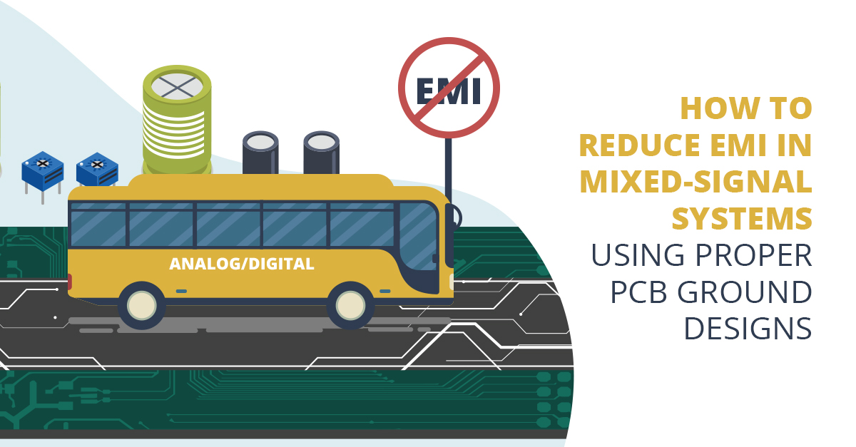
Back when I was living in Philadelphia, I used to drive for an hour to and from work. Those of you who have done long commutes know the sort of road rage even a 5-minute delay can set off. Luckily, Philadelphia's city planning is particularly efficient as a result of William Penn’s careful designs. Were it not for his efforts in traffic efficiency, I’d be spending more time making hand gestures than steering. Sometimes designing a mixed-signal PCB can feel like city road planning. If it is done without forethought it can cause PCB “road rage”, and put out as much electrical “noise” as my car horn. Keeping your board grounded will get you started on the road to an electromagnetic interference (EMI), and rage-free PCB. Here are some suggestions for keeping your board calm and well grounded. Some things discussed below include: a radiated EMI and radiated emission, shielding, EMI noise, and a EMI filter.
Best Practices for Mixed-Signal Grounding
You know that grounding solutions will often need to be specifically tailored for mixed-signal PCBs, but nevertheless, there are several “best practices” that can get you part of the way.
When designing, remember to choose the optimal grounding system; bus wire, grid, or plane.
Bus Wire: For most PCBs with mixed signal systems a bus wire is not a good solution. A bus wire’s impedance can be quite large at system frequencies and this will cause large voltage drops.
Grounding Grid: The grounding grid can be a balanced solution for two layer PCBs that don’t have enough space for a full PCB ground plane, but can’t accept the voltage drops associated with a bus wire. The grid does not have to be a square mesh but should have as much area as possible. A larger area will reduce grid impedance and allow for more trace connections, which in turn shortens current return paths. If you use a grid, take special care to make certain AC/DC return current paths do not cross.
Grounding Plane: Normally the best solution for grounding in a PCB is a full ground plane. Ground plane geometry ensures the lowest possible impedance and often offers the most direct current return paths. Additionally, a full ground plane will have more EMI shielding than a ground grid. Just like with a grid, care must be taken when connecting integrated circuits (ICs) to the PCB ground plane to ensure that return current paths do not cross. As is often the case, the “better” the solution, the more costly it will be. If you’re as frugal as a Quaker, calculating the impedance associated with using a bus wire or grounding grid may be worth your while.
Real grounding is not as easy as on schematics.
If you have any bypass or decoupling capacitors in your PCB design, connecting them directly to the ground plane will help reduce EMI. Grounding these capacitors quickly ensures that return currents have a very short path to complete their loop. If the capacitor connection path to ground is too long, your return currents might take a shortcut and end up where they’re not supposed to be.
Both cities and ICs need good ground
Practical Tips for Mixed-Signal ICs
As you know, mixed-signal systems have complications, but mixed-signal ICs can introduce further complications. Different combinations of these require different solutions, here are some tips when dealing with mixed-signal ICs.
PCBs with a Single Mixed-Signal IC
If you’ve designed audio circuits before you might be familiar with star grounds. When designing a PCB that has only one mixed-signal IC, a star ground can be a great solution. The star ground uses a single point as a reference instead of an entire plane layer. For converters, and some other mixed-signal chips, the manufacturer normally recommends that AGND and DGND pins be connected together outside of the chip, this connection can act as your star ground. If you’re using two separate ground planes with a single mixed-signal IC, you can also tie the two chassis ground planes together at that point. One complication with star grounds is that the connections to the star ground need to be as close to the same length as possible. If that configuration is not practical for your circuit, it’s better to use another ground type.
PCBs with Multiple Mixed-Signal ICs
If your Printed Circuit Board is using more than one mixed-signal IC, the star ground is not practical. This is because you would need to tie the AGND and DGND from each IC together right outside each IC case, all at the exact same point. Not even William Penn could plan that intersection. If you’re building a PCB that has multiple mixed-signal ICs on it, I recommend using a ground plane with gaps to separate return currents, or without gaps and very carefully checked return current paths.
Mixed-signal system grounds require careful layout planning, as return paths need to be checked to reduce EMI and “crosstalk.” Layout planning is very difficult if everything looks the same. I recommend using your PCB design software to color code your components and nets so that you can visually separate AC and DC systems, or pins if you’re working with mixed-signal ICs. CircuitStudio® has documentation showing how to change colors on your Printed Board.
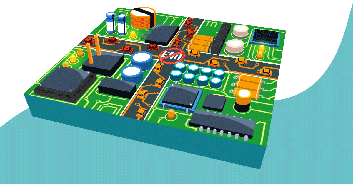
Sometimes congested highways and road rage are unavoidable, but congested PCBs are not. A good grounding layout can reduce EMI on your board, and keep you anger free.
Have more questions about grounding design? Talk to an expert at Altium Designer.