Thermal Relief Design Guide for Your PCB
From relative permittivity to thermal expansion, there are plenty of thermal properties to consider during the design phase. Placing a thermal relief on pads can aid assembly, but this should be considered alongside other methods for managing heat transport in your board. With the right PCB design tools, you can design thermal relief pads for important components and incorporate other important heat management features in your board. Altium gives you these important design tools and much more in a single program.
ALTIUM DESIGNER
A unified PCB design platform that integrates advanced PCB layout features with comprehensive via and pad design features.
Although FR4 is a popular substrate due to its low cost and versatility, it creates problems for thermal management due to its low thermal conductivity. As copper has high thermal conductivity, it can be difficult to heat pads to the right temperature for applying solder, both in some manual processes and in wave solder processes, especially when pads are connected to an internal plane with a via. Managing heat distribution and ease of assembly in your board requires properly designing thermal relief pads in your PCB as well as using other methods to manage heat.
If you’re building a multilayer PCB, then you’ll need to include copper vias to route between the inner layers of your board, and you’ll likely place surface-mount components on copper pads on the surface layer. While every pad and thermal relief device is important for an electrical and assembly standpoint, they can also play a role in heat regulation in your board. With the right PCB design and layout tools, you can easily design thermal vias and thermal relief devices in your board.
What is Thermal Relief Design?
A thermal relief pad provides a way to keep heat confined to a pad for mounting a component to a printed circuit board with solder. The pad for a component normally peaks through the solder mask, allowing solder to placed on the pad during assembly. Some copper is removed from the edge of a thermal relief pad, allowing heat to be confined in the pad when applying solder during assembly.
Thanks to the low thermal conductivity of FR4, heat is easily confined to a thermal relief pad when applying solder. This ensures a strong connection can be formed on a component during manual assembly. This is also important in wave soldering, as a pad without a thermal relief can quickly remove heat from the surface when connected to an internal plane with a via. Choosing where to place a thermal relief on a pad while also including other thermal management methods can ensure that heat is properly managed in the board during operation while ensuring the board can be easily assembled.
Thermal Relief Design and PCBs
The goal in thermal relief design is to remove some copper from around the pad for a through-hole component. You can also use thermal relief design on a pad for a surface-mount component as long as the pad is an in-via pad. In this case, the via functions as the thermal relief device. This is quite important as the copper pad for a surface-mount component needs to maintain some clearance around the edge of the pad, whereas you can easily remove some copper from a through-hole pad without affecting the ability to properly mount the component.
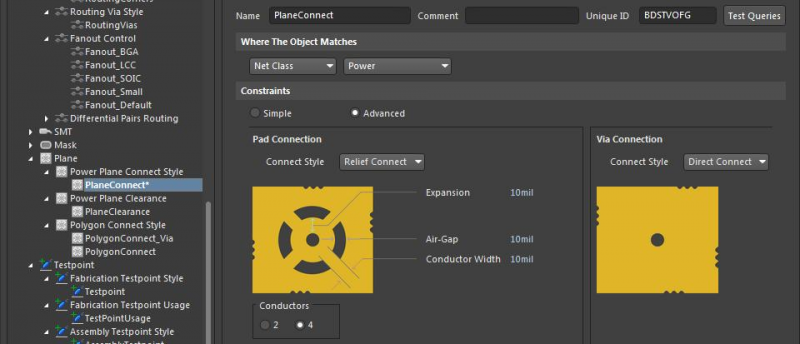
Vias that are not intended for use as pads for through-hole components should not include thermal relief pads. In fact, thermal vias are quite useful for removing heat from active components that generate significant amounts of heat. It is common to place thermal vias on the underside of an active component to regulate its temperature by transporting heat into the board. Placing thermal vias in a thermal relief pad will connect a hole to an internal plane, but spokes and voids are used to restrict the metal area in the internal connection. If you take a look at the image below, you’ll see what a thermal relief looks like. These spokes and voids are important for soldering through-hole components in standard thermal relief pads.
- A thermal relief pad is important both from an assembly and thermal management perspective. Learn more about designing a circuit board with thermal relief pads.
- Your internal ground and power planes are important as part of the connection to thermal vias and your overall thermal management strategy.
- As part of your PCB design software, polygon pour features are important for designing copper regions that can act as heat sinks in your circuit board.

Thermal pad design for power plane connection in Altium Designer
Beyond Thermal Relief Devices: Comprehensive Thermal Management
In some PCBs, high power components and boards that use high current can generate significant amounts of heat during operation, and the low thermal conductivity of FR4 substrates traps this heat in specific areas of the board. There are other methods in addition to the use of thermal vias that can be used to distribute and remove heat from a PCB.
Your PCB substrate and stackup determine many important aspects of your PCB’s performance, including heat transport and management in your board. The thermal resistance of your substrate will determine whether your board can quickly transport heat throughout, leading to more even temperature distribution. When coupled with thermal vias, heat sinks, fans, and thermal relief pads, you can move heat away from components and prevent hot spots from forming in your board while still ensuring solder can be easily applied to your components during assembly.
Other Ways to Aid Heat Management
Using a thermal pad to attach a heat sink, as well as the use of fans, are two popular ways to move heat away from critical active components in your PCB. A ground or power plane on an inner layer in your board will also help move heat laterally throughout a board, helping to produce a more even temperature distribution away from active components. Finally, the thermal conductivity your circuit board substrate determines how quickly your board will conduct heat around a board.
- Unless your board is made from a ceramic material or other alternative substrate material, your standard FR4 board will have low thermal conductivity.
Learn more about selecting the right high thermal conductivity substrate material.
- High power components like bright surface mounted LEDs can benefit from using an aluminum substrate for mitigating heat generation.
- Aside from using alternative substrates and thermal vias, you can help decrease the temperature of your board by mounting a heat sink to planar components with a thermal pad or thermal paste. Learn more about selecting a thermal pad or thermal paste for use with a heat sink.

Your substrate material and your stackup will determine how heat transfers throughout your board
Best Software for Thermal Relief Design
Your thermal relief design features shouldn’t appear in your PCB design software in isolation. You’ll need access to a comprehensive set of via and pad design features that help you define the geometry of thermal relief devices and your layer stack. When these appear alongside your routing features, you’ll have a complete set of PCB design features for thermal relief design.
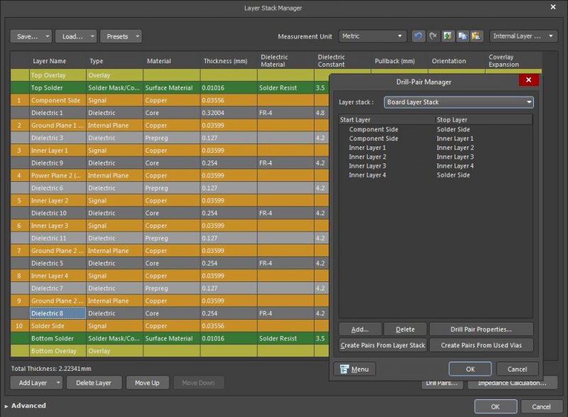
Integrated Thermal Relief Design and Stackup Design in Altium Designer
Altium Designer includes CAD tools that allow you to easily define polygon pours, thermal vias, thermal relief pads, and your layer stack in a single program. You can simplify your PCB design process for thermal management with the via design, pad design, and plane design features.
- Altium Designer’s integrated design environment unifies these important design features and many more on top of a single rules-driven design engine. Defining pad shapes, via shapes, your stackup, and thermal relief devices are easy with Altium Designer. Learn more about the unified design environment in Altium Designer.
- The PCB design rules engine in Altium Designer can help ensure your thermal relief designs are actually manufacturable and will comply with important industry standards. Learn more about the rules-driven design engine in Altium Designer.
- With Altium Designer’s materials stackup library, you can choose a standard substrate material to use as part of a comprehensive thermal management strategy. Learn more about the materials stackup library in Altium Designer.
Thanks to the ultra-accurate CAD tools in Altium Designer, you can easily define your thermal relief pads for important components and design a layer stack that aids thermal management in your PCB. With its huge material library and intuitive stackup manager, you have a complete set of tools for thermal management in a single PCB design program. By integrating your layout, management, and simulation features into a single platform, you’ll have the important design features you need to take control over all aspects of your product.
