Thermal Conductivity and Thermal Management for Printed Circuit Boards
The physical properties of your PCB substrates and copper conductors are the primary factors that determine how it will perform under pressure. Thermal properties, rigidity, dispersion, relative permittivity, and more will affect signal integrity, thermal management, and mechanical performance of your circuit board. When it comes to thermal conductivity, choosing the right substrate can help you combat temperature rise in your board with excessive use of active cooling measures.
With the right substrate material and components layout choices, you can implement a thermal management strategy that can help keep your circuit board temperature low without defaulting to the use of a substrate material with high thermal conductivity. Some simple PCB layout choices will have a big effect on temperature rise and overall thermal management throughout your circuit board. With Altium Designer, you’ll have access to a library of materials that you can use for your substrate, which are accessible within the layer stack manager.
ALTIUM DESIGNER
A unified PCB design package that integrates advanced PCB design and layout features with a comprehensive substrate material library and production planning features.
Your PCB substrate determines many important performance aspects of your printed circuit board. One of the most important material properties, especially in high speed and high frequency devices, is the thermal conductivity of your circuit board substrate. When excessive heat accumulates in your printed circuit board, especially near active components, your components will rise to a high temperature and can wear out quickly, or nearby printed circuit traces and vias can become damaged due to excessive stress.
With the problems created by having a low thermal conductivity, you need to determine the best ways to ensure heat is quickly transported away from active components and evenly distributed throughout the printed circuit board, ensuring a more uniform temperature distribution. External cooling devices like fans can then help remove heat from the board and expel it from the system. Properly compensating for low thermal conductivity requires a comprehensive thermal management strategy that includes proper design of vias, layout of printed circuit traces, placement of thermal reliefs, and even selection of an alternative substrate material.
What is PCB Thermal Conductivity?
As a fundamental property of any material, thermal conductivity (sometimes used interchangeably with thermal resistance) defines the rate of heat transfer between hot a cold regions of your PCB. Active digital components that switch at high speed can generate a significant amount of heat, and the thermal resistance will determine the rate at which heat moves throughout your substrate, components, and copper conductors. Some simple design choices can aid heat transfer between hot and cold regions in your PCB, helping to ensure the temperature distribution in your PCB is more uniform.
Depending on the specific set of components used in your board, the required operating temperature of your board, and the environment in which your board will be used, you may need to implement passive or active cooling strategies to compensate for the low thermal conductivity of most PCB substrate materials. Copper or other metal conductor traces, vias, pads, and reliefs in your PCB will affect heat transfer in your board, but the substrate’s thermal resistance will play an important role in determining the temperature of your board.
Some Design Choices for Thermal Management
Your goal in thermal management is to keep the board’s temperature at a reasonably low value such that your components do not exceed their maximum operating temperature. You should also aim to keep the overall temperature of the substrate below the glass transition temperature (denoted Tg) as this defines the substrate’s transition to a rubbery mechanical state. As heat accumulates in the substrate, it will expand and pull on copper conductors. After repeated thermal cycling over time, your stress will accumulate in copper structures and can even lead to delamination in extreme cases.
You can take advantage of your layer stack to reduce the overall equivalent thermal resistance of your board, allow heat to be more easily transferred away from active components and critical printed circuit traces and vias. This involves choosing the appropriate arrangement of power and ground plane layers in a circuit board. The plane layers are typically copper or another conductor, which provides a low thermal resistance path to remove heat from active components and spread it throughout the board.
Using copper thermal reliefs and thermal pads on active components also helps remove heat into a copper plane or a heatsink, respectively. Once heat is transferred into a heatsink, it can be removed by taking advantage of airflow across the surface of the heatsink. When combined with proper stackup design and substrate material selection, you can reduce the number and/or size of active cooling measures you need to implement during PCB design.
- As part of a passive cooling strategy for active components, you’ll need to decide whether to use a thermal pad or thermal paste to bond a heatsink to larger active components. Learn more about thermal pads and thermal paste.
- Your layer stack also determines the effective dielectric constant of traces in a signal layer, which in turn determines the impedance of a trace in a printed circuit. The right layer stack can help prevent signal integrity problems and forms the cornerstone of a heat management strategy.
- Every active component acts as a heat source. If you have a large number of active components that operate at very high speeds, then you may have no choice but to include some active cooling components in your PCB.
Learn more about working with active cooling components in your PCB layout.

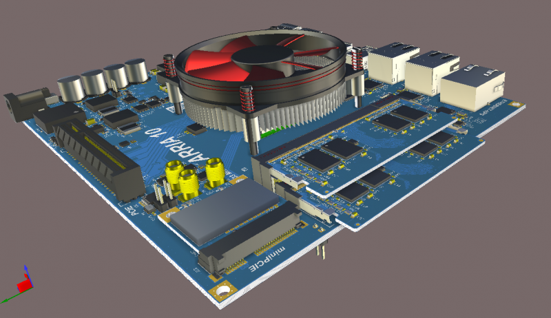
3D view of a multi-board system with a large cooling fan
Alternative Substrate Materials for Thermal Management
Defining a stackup is just one important aspect of designing your board. The materials used in your stackup will help determine the overall thermal resistance and resulting heat transfer rate in your board. The thermal conductivity of common PCB substrate materials ranges from 0.3 to 0.6 W/mºC. This is much lower than the accepted thermal conductivity of copper (386 W/mºC).
In the event that your printed circuit board will be deployed in a high temperature environment, you can move heat away from hot spots in your circuit board by using a substrate material with higher thermal conductivity. Some common alternative substrate materials are ceramics, which have very high thermal conductivity. Another option is metal core PCBs, where the central core layer of the board is some metal with high conductivity.
A Comparison of PCB Substrate Materials
Ceramic materials are more expensive from a manufacturing standpoint, but they provide anywhere from 20 to 100 times higher thermal conductivity compared to FR4. Metallic core LEDs provide similar thermal conductivity as well as a mechanically stronger overall structure. Any of these options are an excellent choice for moderately high frequency applications. For much higher frequency applications (e.g., 10’s of GHz), PTFE laminates with metal planes and core may be a better choice from the perspective of balancing dielectric losses and thermal management.
- Compared to standard FR4, ceramic materials have much higher thermal conductivity and are ideal for use in higher temperature environments.
- If you are using high power components like bright surface mounted LEDs, you can benefit from using an aluminum substrate.
- Aside from ceramics and metallic substrates, your substrate materials will determine other important properties of your circuit board beyond thermal conductivity.Learn more about selecting the right substrate material.

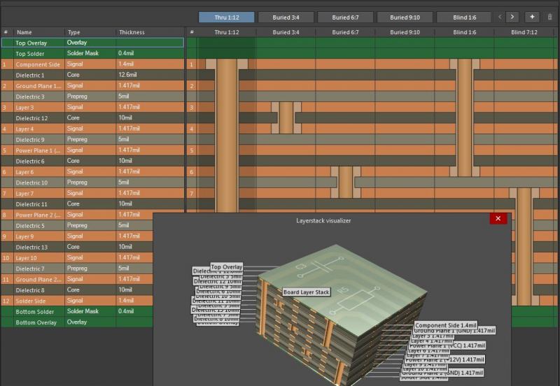
Stackup design in Altium Designer
Best Software for PCB Thermal Conductivity Management
Unless you have access to an integrated design package, you’ll need to work with multiple programs to create your schematics, layout your printed circuit board, simulate its behavior, and plan for manufacturing. The best software for PCB thermal conductivity management integrates these tools into a single program along with a huge components library, giving you the ability to design copper thermal reliefs and vias, implement passive or active cooling measures, and define a thermally conductive layer stack.
Integrated Layer Stack Design and Material Selection in Altium Designer
Altium Designer includes a top-notch layer stackup manager that allows you to customize your substrate electrical and thermal properties for use with unique materials. This simplifies your PCB design process as you can incorporate any material into your stackup as part of a comprehensive heat management strategy. Your stackup is then immediately defined in your PCB layout editor and the material properties are included in your simulation tools.
With the material library in Altium Designer, you can easily select from a large number of common materials for use as your core, prepreg, and laminates. You can also define your plane and signal layers as part of your stackup, giving you a complete basic circuit board for use with components layout and routing. You can then take your design data and immediately import it into your simulation and production planning tools. You’ll be able to move through the entire PCB design process with Altium Designer.
- Altium Designer’s integrated design environment unifies your important design features on top of a rules-driven design engine. Defining your stackup, arranging components, and routing are easy with Altium Designer. Learn more about Altium Designer’s unified design environment.
- Altium Designer contains a complete materials stackup library for use as any PCB substrate. You’ll be able to easily define your layer stack and material properties for niche materials in Altium Designer. Learn more about the materials stackup library in Altium Designer.
- Working with a power density network analyzer helps you examine power integrity problems and potential hot spots in your board. Learn more about the PDNA extension for Altium Designer.
With the ultra-accurate CAD tools in Altium Designer, you can easily place components, as well as add thermal reliefs and copper pours, to your printed circuit board. Add to this the material library, stackup manager, and PDNA extension, and you have a complete set of tools for thermal management in a single PCB design program. You can implement the right strategy to combat temperature rise in your PCB and transfer heat away from critical components in your PCB.
Altium gives you the resources you need to design your printed circuit boards for use in any application. You’ll have access to the AltiumLive forum, podcasts and webinars with industry experts, an extensive knowledge base with plenty of design tips, and design tutorials. No other PCB design software company give you this level of support.
Altium Designer has set a new standard in circuit board design tool integration and analysis. By integrating your layout, schematic design, data management, and simulation features into a single platform, you can easily pass design data between these important design features and take control over all aspects of your product.
