PCB Impedance Calculator and Stackup Design in Altium Designer
There are many demands placed on PCB stackup design. High-speed designs carry a requirement for controlled impedance, crosstalk control, and the need for interplane capacitance. Impedance in your traces becomes a critical parameter to consider during stackup design for high-speed PCBs, but the stackup will also influence crosstalk susceptibility and sheet capacitance between ground and power planes. While you can work out many of these details by hand or with a circuit design program to model impedance in your board, the best PCB design tools give you more sophisticated ways to design for controlled impedance.
Instead of using an online PCB impedance calculator to determine the impedance of each trace in your PCB, Altium Designer incorporates PCB impedance calculations as part of your stackup design process. The integrated field solver in Altium Designer's layer stack manager and routing features can help you manage impedance throughout your board. If you're ready for a simplified, seamless PCB impedance calculator for your high-speed design, look to the Layer Stack Manager and routing features in Altium Designer.
ALTIUM DESIGNER
A rules-driven PCB design platform with a built-in PCB impedance calculator for high-speed PCB design.
In the early days of circuit board design and fabrication, logic circuits were so slow that the only concerns were making connections between logic or discrete parts and providing a path for DC power to each part. All a designer needed to do was provide enough signal layers for all wires and enough copper in power paths to deliver DC power with minimum sag or droop. The glass cloth in the laminate and prepreg did not matter, nor was the resin system important. The goal was the lowest priced PCB that would stand up to the soldering process.
Today, logic families in ICs are fast enough that problems such as reflections and crosstalk are prominent in any high-speed board unless an impedance profile is properly engineered for interconnects. ECL was the first logic family that made these problems prominent. Few of the early engineers designing with TTL and CMOS had any understanding of how to design a PCB with controlled impedance. Once the requirement for specific impedance values was realized, engineers would simply demand the fabricator deliver PCBs with a known impedance, usually 50 Ohms.
Since impedance control is so important, designers need to perform impedance calculations when they design the PCB stackup. Although the layer arrangement in the PCB stackup is critical for ensuring impedance goals are met. There are calculators on the internet that can give you some accurate results, but they cannot account for dispersion throughout the signal bandwidth, nor can they consider things like copper roughness or etching along the surface of a copper trace. If you have a PCB impedance calculator integrated into your design tools, you can quickly determine impedance for any trace geometry as you create your stackup and start your PCB layout.
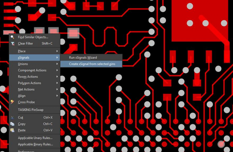
You can control the impedance of all these trace by designing the right stackup and trace geometry.
How to Calculate PCB Trace Impedance in Your Stackup
The impedance of the traces in your PCB depends on their geometry, the PCB core/prepreg material used in the stackup, and the layer arrangement. Edge-coupled, embedded, and offset trace arrangements all have variations in their impedance values, and you’ll need design software that can account for the impedance of these different geometries. These tools should also have utilities to model copper roughness and dispersion.
Unfortunately, online PCB calculators and some analytical formulas cannot account for these points, so you won't have the ability to adjust for roughness, dispersion, or etching in these models.
PCB Impedance Calculations With IPC-2141 Formulas
A number of equations are used to define and calculate various design parameters in PCBs, just like any other area of engineering. The equations for trace impedance must account for everything from the substrate dielectric properties to the geometry of your traces. The most cited formulas for microstrip impedance and stripline impedance are the IPC-2141 formulas:
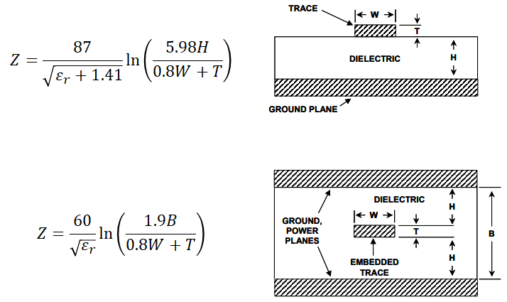
IPC-2141 microstrip and stripline impedance formulas
These formulas are known to produce up to 7% error in certain frequency ranges, which is unacceptable for high speed and high-frequency applications, as well as and in multilevel signaling protocols that have GHz bandwidths. Alternative tools are needed to determine PCB trace impedance.
Wadell's Impedance Equations
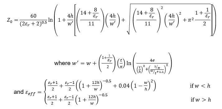
A much more accurate set of equations that are suitable for PCB impedance calculations is Wadell's equations. These impedance equations provide more accurate calculations, although inverting them to get the required width and laminate thickness needed to reach a specific impedance value is more difficult. The trace impedance determined with Wadell’s equations is more accurate, reaching less than 1% error.
For microstrips, Wadell's impedance equations are:
For symmetric striplines Wadell's impedance equations are:
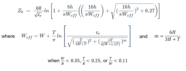
The next step in using these equations is to determine how the layer arrangement in your board will determine impedance, and select the geometric parameters you want to use. You will also need to select the dielectric substrate material you will use in your PCB layout as this will determine the dielectric constant, which also appears in the impedance equations shown above.
For other arrangements, like coplanar lines, offset striplines, or waveguides, more sophisticated techniques are needed. However, once you determine the layer arrangement you need, you can use a field solver to determine the width required for a specific impedance in your PCB layout.
How Your PCB Stackup Determines Impedance
The figure below shows an example of the tradeoffs between routing layers and power plane capacitance for a 10-layer PCB (bold lines are plane layers, P = prepreg, L = laminate). The stackup on the left side has six signal layers, but it only has one pair of planes closely spaced. This is good for routing space, but not so good for power delivery if there is a need for interplane capacitance. The stackup on the right has only six routing layers, but it now has two sets of plane pairs. This is good for interplane capacitance, but not as good for routing space.

Two example stackups for 10-layer PCB.
In both cases above, all the signal layers are mated with planes across pieces of laminate except the two outer layers. When the power and ground planes are closer together, they provide more interplane capacitance, thus the two planes act like a large decoupling capacitor. If the outer layers are to be used for controlled impedance traces, allowance must be made for the fact that their tolerance will not be as good as the buried signal layers.
Getting your stackup just right means that you need software that lets you fully customize your layer stack, right down to selecting the appropriate dielectric constant for your board layers. A stackup manager that links to material library helps greatly as you can choose from common board materials when planning your stackup. You can select the right thickness for your layers and define the best trace arrangement for your board. When determining the impedance of your traces on these signal layers, your PCB impedance calculator needs to account for these varying plane/signal arrangement and layer thicknesses.
The PCB Impedance Calculator in Altium Designer
The Layer Stack Manager in Altium Designer can be used to easily arrange signal and plane layers in a PCB stackup and determine the impedance of traces in each layer. This tool includes an industry-standard field solver that is built into your PCB layer stackup. You won't need to manually calculate trace impedance with formulas or an external application, everything happens in Altium Designer as you build your PCB stackup.
- Your stackup affects your trace impedance, and you can take advantage of this to control impedance throughout your board.
Learn more about your layer stackup and how it affects trace impedance. - Any impedance calculation needs to account for dispersion in the dielectric substrate in order to produce accurate results at any frequency.
Learn more about dispersion in FR4 and other substrates. - If you must terminate certain elements in your PCB, there are a number of standard termination methods that you should use.
Learn more about integrated field solvers in your PCB design software.
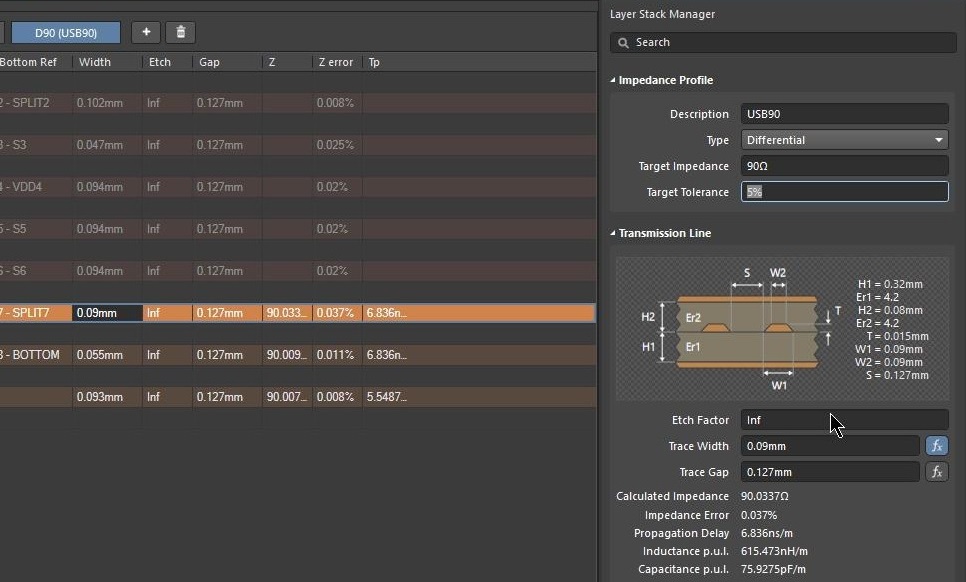
PCB stackup editor in Altium Designer with an integrated electromagnetic field solver.
PCB Impedance Calculator in Your Layer Stack Editor
The value of H in the above equation accounts for your layer spacing in your stackup, which plays an important role in determining the impedance seen by your signals, as well as some other important aspects of high-speed circuit board design. The layer arrangement and separation in your stackup affect three important aspects of high-speed PCB design:
- Interplane capacitance: This is critical for maintaining stable power in high-speed devices. Placing power and ground planes on adjacent layers with thin separation provides high interplane capacitance, as mentioned above.
- Parasitic inductance: The loop inductance for traces determines susceptibility to inductive crosstalk. When the layer spacing is smaller, the loop inductance is also smaller.
- Coupling between traces: Traces will couple inductively and capacitively, and the layer spacing plays a role in determining this level of coupling. This, in turn, determines the values of even, odd, and differential impedance.
The dielectric constant of your substrate also determines your trace impedance, as shown in the above equation. The dielectric properties of your substrate also need to be included in your impedance calculations and PCB stackup design. This is because the dielectric constant varies with frequency, which will affect coupling, crosstalk, and trace impedance.
Accurate Impedance Calculations vs. Frequency
A question that often arises is, at what frequency impedance calculations should be performed? Modern ICs have rise times well below 1 nanosecond and bandwidths extending out to GHz frequencies. Bandwidth limiting effects in a channel include the load capacitance, the Nyquist frequency of receiver, and the loss spectrum (composed of frequency-dependent dielectric loss and copper roughness loss). Getting the right impedance requires dispersive models be built into your impedance calculation tools so that the broad bandwidth of digital signals can be accounted for in a PCB impedance calculator.
One of the reasons that PCB fabricators do not get impedance calculations right is that they often use the typical value of dielectric constant listed on the data sheet which is usually the 100 MHz or 1 GHz value. If the dielectric constant varies with both frequency and resin content where does one obtain the correct values? The best PCB design software integrates these capabilities using data in a materials library, which will account for dispersion in the dielectric.
Because of these complications involved in accurate impedance calculations and PCB stackup design, your impedance calculator needs to consider trace geometry and dispersion simultaneously. This is why the best PCB trace impedance calculators are built on an integrated 3D field solver. This type of PCB impedance calculator provides the most accurate results for any geometry.
- Your stackup affects your trace impedance, and you can take advantage of this to control impedance throughout your board.
Learn more about your layer stackup and how it affects trace impedance. - Any impedance calculation needs to account for dispersion in the dielectric substrate in order to produce accurate results at any frequency.
Learn more about dispersion in FR4 and other substrates. - Impedance calculations, propagation delay, reflections, and crosstalk are easy with the integrated field solver in Altium Designer.
Learn more about Simberian’s integrated field solver in Altium Designer.
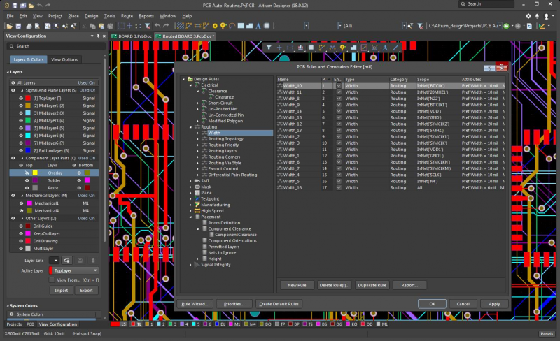
Defining rules and constraints for a high-speed PCB in Altium Designer.
Unifying Signal Integrity Tools in a Rules-Driven Environment
Working with software that includes impedance calculations as part of your design rules allows you to automatically check that the impedance in your traces is properly controlled. You won’t have to manually check every single trace. Instead, you can specify the calculation you need for your trace arrangement and substrate, and your design tools will automatically check your routing to ensure controlled impedance throughout your printed circuit board layout.
The rest of the PCB design industry still separates your critical design, management, and verification features into separate programs with different workflows. When you need to control the impedance of single-ended or differential traces in your PCB, you’ll have to use multiple design tools that each focus on a different aspect of your final PCB. Working with design software that separates tools into different windows reduces your productivity, making it difficult to address what should be simple design issues.
Your design tools, design rules, component models, and simulation packages should be placed in an integrated environment with a consistent workflow. Features in this environment are all accessible from a single program, and new features can be easily added to your design software as extensions. This is exactly the type of design environment you’ll find in Altium Designer.
Impedance Calculations and PCB Stackup Design in Altium Designer
Impedance calculations can be done by hand, but you’ll get the most accurate results for any frequency and geometry when your trace impedance calculator is integrated with your PCB design tools. This type of unique integration of multiple design tools is only possible when you work in a fully unified design environment. Altium Designer is the only PCB design software package that runs on a heavily rules-driven design engine, and all your design verification features interface with your design tools in a single interface.
- At the core of Altium Designer is a rules-driven design engine. This unique software architecture allows all your design tools to communicate with the same data model.
Learn more about the rules-driven design engine in Altium Designer. - Your layer stackup determines your trace and PDN impedance throughout your board. Your layer stack manager should allow you to customize your layer arrangement and define the impedance required for your application.
Learn more about the advanced layer stack manager in Altium Designer. - Once your PCB stackup is created and you've created impedance profiles for your traces, the Altium 365 platform lets you share your designs with collaborators and manufacturers.
Learn more about sharing your PCB project data with Altium 365.
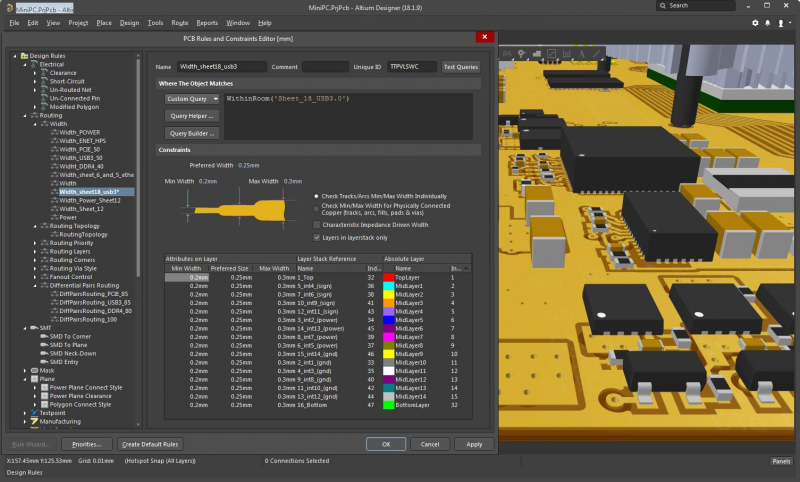
Defining trace geometry and impedance control tolerances as design rules in Altium Designer
If you’re tired of working with separate design tools in different programs, you need to use Altium Designer’s unified circuit board design platform. You can access all your important design tools for high-speed PCB design and signal integrity analysis in a single program. Instead of guessing at best trace geometry for your next PCB, Altium Designer can help you get it right the first time with integrated impedance calculations and PCB stackup design tools.
Altium Designer on Altium 365 delivers an unprecedented amount of integration to the electronics industry until now relegated to the world of software development, allowing designers to work from home and reach unprecedented levels of efficiency.
We have only scratched the surface of what is possible to do with Altium Designer on Altium 365. You can check the product page for a more in-depth feature description or one of the On-Demand Webinars.
