Getting Your Layer Stack Right
Download the PDF to keep learning offline
An improper layer stack in your PCB design is one of the most common errors leading to fabrication failures and rejects.
Every multilayer circuit board needs a precise PCB stack-up and accurate layout before it can be sent for PCB manufacturing. When you have the right set of circuit board design tools, you can turn your stackup into a real PCB layout and prepare the documentation your fabricator needs. The multi-layer PCB troubleshooting tools in Altium Designer make it easy to check your layout against design rules and prepare your board for full-scale fabrication. There’s no reason to guess at the configuration of your circuit board layers anymore.
TOPICS IN THIS SOLUTION
Creating a Multi-Layer PCB Configuration
Designing a modern printed circuit board, regardless of its layer count, can be a challenge. Everyone wants more electronics and functionality stuffed into their designs, forcing designers to route and layout components with higher density and higher signal speeds. Creating multilayer PCBs for rigid, rigid-flex, or flex designs requires state of the art design and multilayer PCB troubleshooting tools to create the circuit board layer stackup your designs need.
PCB designers might rely on input from their PCB manufacturing vendors for their layer stackup information, but the right set of PCB design tools can help you take manufacturing information and troubleshoot complex designs. When you use Altium Designer, you can create a precise PCB stack-up for your multilayer circuit board and prepare it for manufacturing. The built-in design rule creation and management features point out design errors as you create your PCB, giving you everything you need to create a high-quality multilayer circuit board in a single program.
Creating a Multi-Layer PCB Configuration
Creating a printed circuit board requires multiple design features so that all aspects of a new circuit board can be included in a PCB layout. The number of layers in a PCB is dependent on the amount of circuitry on the board and the electrical requirements of those circuits. Very subtle changes to the materials used for the dielectric layers can create a huge difference in circuit performance, and your PCB layer configuration must take all of this into account.
With the CAD tools and stackup design features in Altium Designer, you’ll have the tools you need to engineer your stackup. You can create the stackup you need to accommodate your net count and routing topology, as well as supply power and ground points to your components. These features integrate with Altium Designer’s design rules to keep your routing width and spacing accurate for your signalling standard. Take control over every aspect of your printed circuit board design and ensure your design can be manufactured error-free.
Create Your PCB Layer Stackup in Altium Designer
Once you’ve determined the routing and layout requirements for your circuit board, you can create your PCB stackup with the Layer Stack Manager in Altium Designer. Once you create your stackup, you can easily control layer views in the PCB Editor window. These features make circuit board design and printed circuit routing quick and easy.
- Board thicknesses may be standardized by many manufacturers, but you still have freedom to design your PCB layer stack as you see fit.
- Rigid-flex and flex circuit board designs have their own stackup and routing rules that need to be followed to ensure a board can be manufactured successfully.
Learn more about printed circuit layer stack design for flex and rigid-flex boards.
- The ground plane in a multilayer PCB stackup is a critical feature to be designed to ensure power integrity and signal integrity.
Learn more about placing ground planes in your multilayer circuit board.

The view configuration tools in Altium Designer give you full control over your multilayer PCB.
Advanced Multilayer PCB Design in Altium Designer
Altium Designer’s Layer Stack Manager helps you create a precise configuration for a multi-layer circuit board. This becomes critical for ensuring signal integrity in your printed circuit design as you need to control return paths, control impedance, and ensure power integrity. Layers can be difficult to manage when paired with pad and pin placement, components and traces, copper and solder flow, and schematic generation with multilayer PCBs.
Fortunately, Altium Designer makes it easy to define all aspects of your printed circuit layer stackup. When you need to troubleshoot your multilayer circuit board layout and routing, the design rules in Altium Designer take the information you define in the Layer Stack Manager to evaluate your layout. The ease of using the Layer Stack Manager and setting design rules in Altium Designer helps you stay productive and design to your specifications.
Engineer Your Multilayer PCB Stackup with Altium Designer
With the advanced functionality built into Altium Designer’s Layer Stack Manager, you can ensure your layout and routing fits within your DFM rules and impedance specifications. Placing power and ground planes in your circuit board in the right spots allows you to control impedance as well as ensure signal integrity in your PCB. Altium Designer gives you all the tools you need to engineer your printed circuit layer stack.
- There are many variations of a single PCB stackup, and correct placement of power and ground planes helps ensure your board functions as intended.
- A complex circuit board layer stackup will include multiple power and ground planes, which will determine whether you can control impedance at the desired values.
Learn more about impedance control by engineering your layer stack.
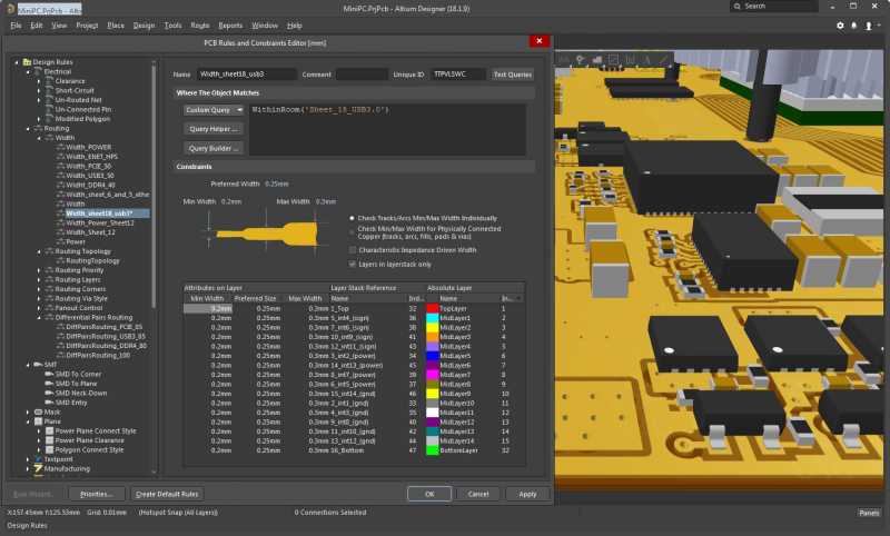
- The Layer Stack Manager in Altium Designer interfaces directly with your PCB design rules, allowing you to take full control over routing in your circuit board.
Learn more about using the Layer Stack Manager and your design rules in Altium Designer.

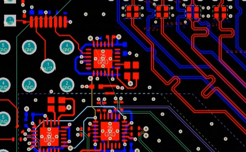
Routing in a multilayer PCB is easy with the layout tools in Altium Designer.
Rules-driven Design for Multilayer PCBs in Altium Designer
Checking your routing and layout in a multilayer PCB doesn’t have to be a manual process. The rules-driven design engine in Altium Designer is ideal for ensuring your new circuit board complies with important DFM checks and that you’ve properly routed your multilayer PCB. You can ensure your circuit board passes in-house Q&A inspection before being sent to a fabrication house.
In order to guarantee your PCB fabricator has the required information to order layers properly, you need to generate PCB assembly drawings and manufacturing files directly from your design data. The circuit board manufacturing documentation features in Altium Designer allow you to create these important files directly from your design data. These manufacturing and design features are all accessible in a single application, giving you a complete set of tools for PCB design and fabrication.
Design and Manufacture Your Multilayer PCB with Altium Designer
Altium Designer gives you much more than a set of multilayer PCB troubleshooting tools. You’ll have a complete set of component supply chain management tools and simulation features to help you source and evaluate your design. Everything you need to design, simulate, and fabricate a high-quality circuit board is included in Altium Designer.
- Altium Designer makes multilayer PCB design easy with advanced layout and routing tools in a single program. You’ll also have everything you need to prepare fabrication and assembly drawings for your multilayer board.
Learn more about the integrated PCB design interface in Altium Designer.
- The Layer Stack Manager in Altium Designer makes planning your PCB stackup easy. The Layer Stack Manager includes an integrated field solver for accurate impedance calculations and copper roughness modeling.
Learn more about the integrated field solver from Simberian in Altium Designer.
- Complex multilayer PCBs can require a collaborative design process. Altium Designer makes this easy by integrating with the Altium 365 platform. You can share designs with anyone and work from anywhere when you use Altium Designer and Altium 365.
Learn more about sharing and collaboration with Altium Designer and Altium 365.

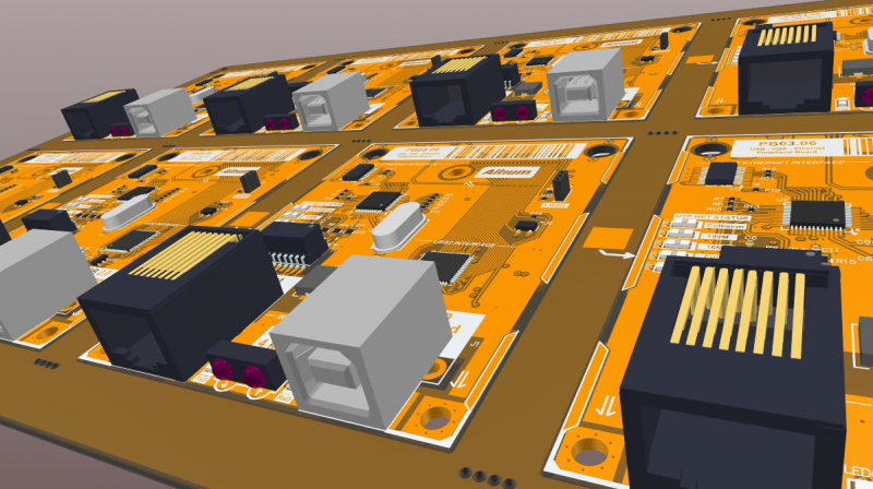
This multilayer PCB is ready for PCB manufacturing and assembly.
Whether you’re designing a simple two-layer board or a complex multilayer PCB, you need the complete set of design tools found in Altium Designer. Create your circuit board, ensure signal integrity, and prepare your design for manufacturing in a single application with Altium Designer.
Altium Designer on Altium 365 delivers an unprecedented amount of integration to the electronics industry until now relegated to the world of software development, allowing designers to work from home and reach unprecedented levels of efficiency.
We have only scratched the surface of what is possible to do with Altium Designer on Altium 365. You can check the product page for a more in-depth feature description or one of the On-Demand Webinars.
