PCB Layout for an LM358 Op-amp Circuit and Module
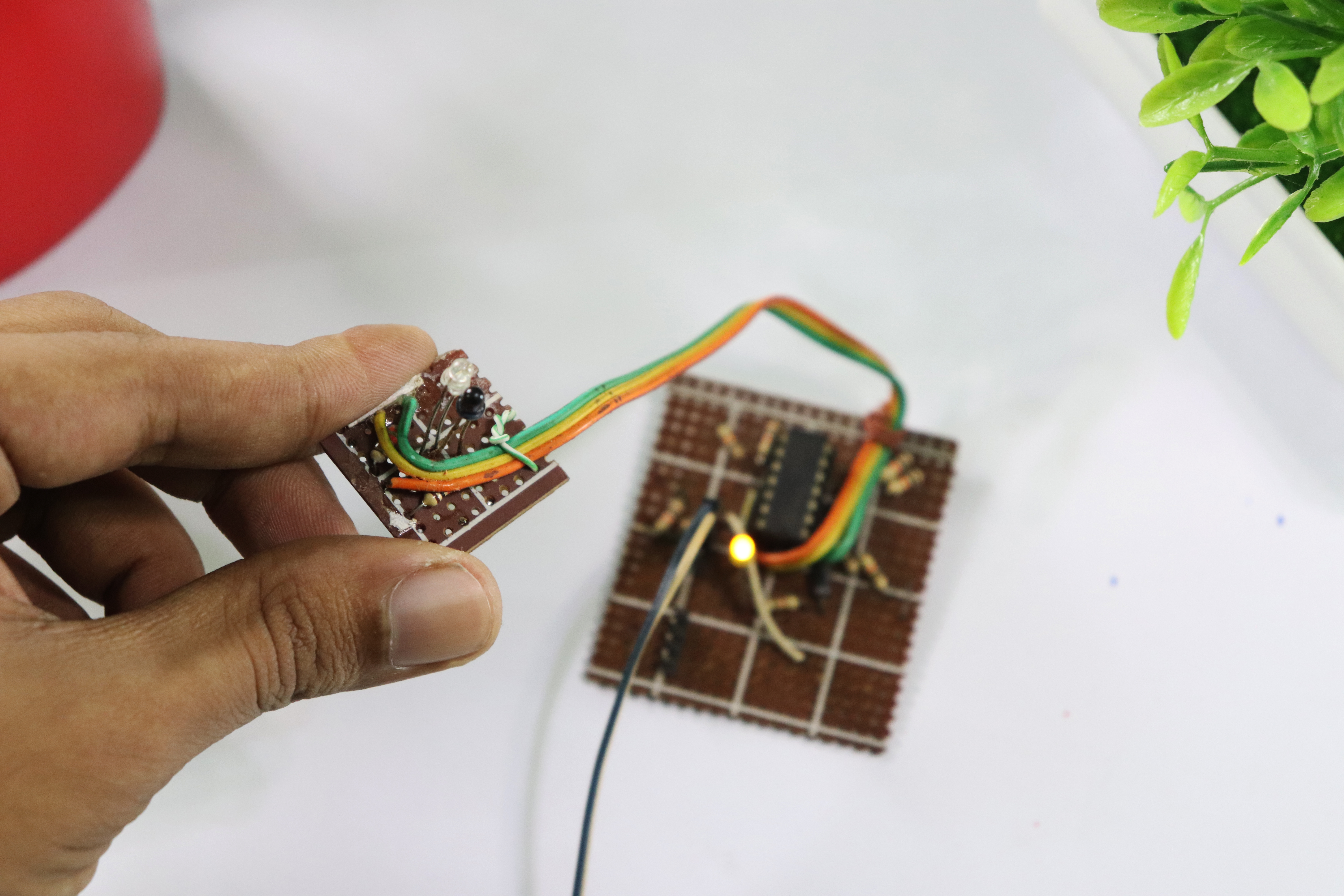
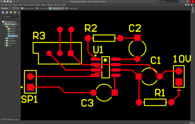
In a previous post, we focused on making a simple active amplifier using the TI LM386 op amp. We’ll be continuing from the end schematic of that tutorial, then walking through the process to create a finished PCB layout in Altium Designer®. This layout contains an LM358 op-amp circuit that runs at audio frequencies, as well as a number of other components. The component count is low enough, and the frequency range is low enough that we can place all the components on a single layer. The finished version of our PCB layout will look something like this:
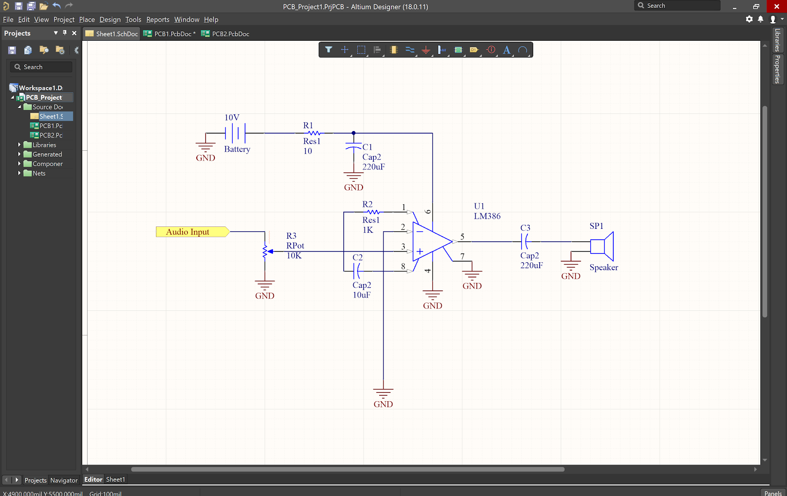
Our LM358 Op-amp Circuit Schematic
Below is the schematic we’ll use to get started on our PCB layout, but with one minor correction: the speaker designator has been updated to SP1. In the image below, we’ve already added the schematic to a new PCB project, and we’re now ready to add a blank PCB into the project to get started on the layout.
Create a New PCB File
Now that the schematic is finalized, you’ll want to add it to a new PCB project and create a blank PCB layout. Go to the Navigator panel, right-click the PCB project file, and select Add New to Project ⟶ PCB. After opening the new file, you should see a blank PCB document:
At this point, I usually like to turn off the ‘automatic room generator’ option before importing components into a new PCB. This will get rid of the predefined red box that you’ll see after you import components into a new PCB file. Note that this is not required, but it does make things easier if you don’t feel like having components grouped into rooms while creating your layout. To turn off this option, navigate to Project ⟶ Project Options ⟶ Class Generation then unselect Generate Rooms.
Import Schematic Components
Once you’ve saved your project with the new PCB file, and there will be no other changes to your schematics, you’re ready to import your components. After the PCB manufacturer project is saved, navigate to Design ⟶ Import Changes from [PCB Project].prjPCB. You’ll see the Engineering Change Order screen, which will allow you to select which components you want to import into the PCB layout:
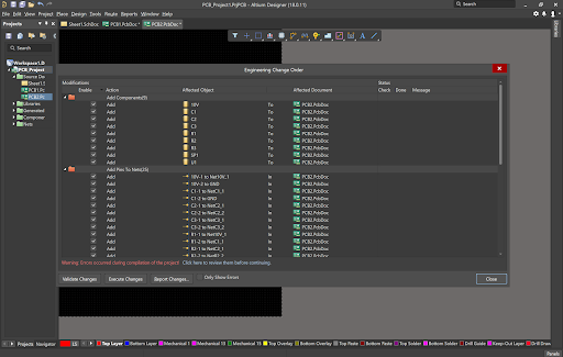
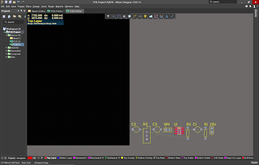
If your PCB layout currently doesn’t contain any components and you just want to import everything, simply select Execute Changes, then Close. For more complex projects, you might want to click through different groups of components to import so that you can work through different sections of your PCB layout. Otherwise, you can just select everything, and your components will be placed in the lower right area of your PCB document:
Arranging Components
From here, you can simply drag the selection box over all the components and drag them anywhere in your circuit board space. The initial placement of components isn’t so critical; you’ll be moving them around so that you can easily route traces around the board. You can start rearranging each component following the routing guidelines as best as you can until you reach a placement configuration you think will work.
There are two helpful features that will help you quickly arrange components in the board as you create your PCB layout:
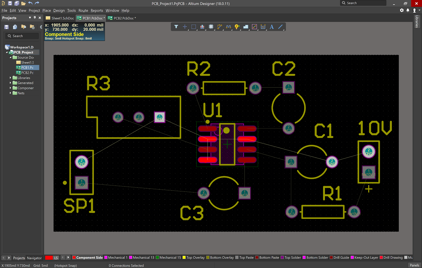
- Show nets: One easy way to see which connections will be routed together with traces is to show nets in the PCB Editor. The nets appear as white lines running between different pads on your PCB footprints. In the PCB Editor window, hit the N key and select Show Connections ⟶ All to show nets.
- Component rotation: A feature that saves me a lot of time is a shortcut for component rotation. Rather than going into the Edit menu to rotate a component, you can hit the spacebar while dragging a component. This will rotate the part 90 degrees while you drag the component.
- Net highlighting: In a simple board like this, you probably won’t need net highlighting, but it becomes very useful when your layout gets dense. This gives you a simple way to track connections throughout your PCB layout.
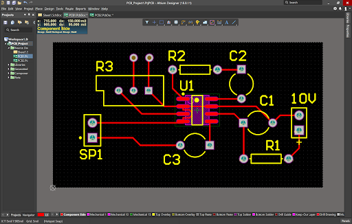
The arrangement below shows the finalized component arrangement that I’ll use for this LM358 op-amp circuit. Here, you can see the nets connecting pins/pads on different components.
Changing Board Size
Now that the components have been arranged in the board, it’s time to set the appropriate board size for this PCB. To change the board size (the black background), navigate to View ⟶ Board Planning Mode. Once you see a green board, navigate to Design ⟶ Redefine Board Shape. You’ll be able to trace out a board of any size around the above components. The circuit board corner defaults will be set to a 45-degree angle. To change this, press Shift + Spacebar to toggle through the various options. I usually stick to 90-degrees.
Set the Origin
The origin is important in any CAD document as it defines where different all other objects on the board will reside. Your manufacturing documentation, particularly your Gerber files, will need to be designed to correspond to the same origin in the board. Since you have modified the component locations as well as the board size, it is good practice to place an origin point at an intuitive location.
The typical practice is to use Cartesian coordinates and place the origin at the bottom-left of the board. This means every other location on the board will have positive x and y position values. To set the origin, simply navigate to Edit ⟶ Origin ⟶ Set and place it wherever your heart desires.
Set up Design Rules for Trace Routing
After you define the board size and place the origin, you can set up design rules needed to start routing your traces from pin to pin. To establish any trace rules, such as default trace width, annular ring requirements, etc., navigate to Design ⟶ Rules and create, delete, or modify any rules you wish to implement upon beginning your tracing process. For this tutorial, you’ll leave all rules as they are as we are working with low-speed/low-frequency signals.
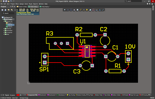
Once these design rules are set up, you can start routing traces. Altium Designer includes an Autorouter tool that might produce some useful results in a simple board like this, or you can use the interactive routing features. Just as in board boundary creation, you can press Shift + Spacebar to toggle through various corner shapes. I like to leave this set to the 45-degree default corner option since it’s the one that most closely resembles a Tron-like configuration. The fully routed LM358 op-amp circuit layout is shown below:
Adding Vias to Your PCB Project
Since this example requires input from an audio source, you’ll need to add in a few very basic ports for a source to solder to. This could be a specialized connector or something simple like a pin header. One simple way to add a pin header or two solder points for external wires is to add large plated vias to your board.
You can use the default via template to place vias in your PCB layout. Navigate to the upper toolbar and select Place Via and simply place it wherever you choose. You may have to designate a Net to each via before a trace is allowed to connect, particularly if this is for a power connection. To do this, double-click the corresponding via, and under Net select which net you will connect to. In our example, I placed them in a convenient location for our user to access and added traces directly to them:
A PCB Emerges
After these steps are completed, you can start preparing Gerber files, assembly documents, and other deliverables for a fabricator to start manufacturing your board. You can design plenty of other PCB for a range of applications thanks to the huge range of design and layout tools in Altium Designer.
If you would like to know more about the Altium Designer platform and how it can greatly assist in your design, feel free to talk to an Altium Designer expert today.
