Thermal Via Management for PCBs
An active component can act like a powerful heat source in your board, ultimately determining the equilibrium temperature in your PCB. Frequent cycling between high and low temperatures, as well as running active components at high temperature for extended periods of time, will reduce the longevity of your system and can lead to premature component or conductor failure. These heat transfer and temperature problems can be prevented with a thermal management strategy.Your thermal management strategy will likely need to include strategic placement of thermal vias, which aids heat transfer away from high power active components. Some examples include high speed processors and power electronics. If you know how to manage thermal vias and strategically place them near your high power components, you can help reduce the temperature in your board and eliminate hot spots.
With the design tools in Altium Designer, you can implement a thermal management strategy in your circuit board that includes thermal vias, pads, heat sinks, active cooling, and even high conductivity substrates with custom stackups. Here is what you need to know about working with thermal vias in your next circuit board.
ALTIUM DESIGNER
A unified PCB design platform that integrates advanced PCB layout features with comprehensive via and pad design features.
Thermal management problems in any circuit board can lead to hot spots in various locations in the board. These hot spots tend to accumulate near active components as these components generate a significant amount of heat. Due to the high thermal resistance of FR4, it is difficult to transport heat away from these hot spots on the component layer. There are some important thermal management strategies any designer can implement in their circuit board to help mitigate problems associated with hot spots.
As copper has high thermal conductivity, you can place copper elements in strategic locations to help prevent excessive temperature rise near active components. Placing copper elements near active components aids heat transfer away from active components as this will provide higher effective thermal conductivity in your substrate. Among the various methods for thermal management, strategic placement of thermal vias in addition to other methods will help remove heat from important components.
With the right circuit board layout tools, you can design and implement an effective thermal management strategy that includes design of thermal vias, a heat sink for each high power active component, and active cooling measures that do not incur significant signal integrity or EMI problems. Altium Designer includes these important layout tools and much more, allowing you to combat temperature rise in your circuit board and ensure the temperature distribution is more even throughout your circuit board.
What is Thermal Via Management?
Active components like power electronics devices, high speed processors, and high frequency components will most likely need to include thermal vias. Many components, such as those in QFP packages, include a heat sink pad on the bottom of the component. When a thermal interface material is attached to the bottom of the component, you can provide a low thermal resistance for dissipating heat into the substrate.
As many boards are placed on FR4, which has high thermal resistance, heat accumulates near the bottom of the component and leads to a large temperature increase. Once heat is transported to the substrate, it tends to remain trapped near the surface layer, causing a significant temperature increase. The temperature differential between uncooled active components and other areas of your circuit board can reach near 30 Celsius. Thermal vias in contact with an active component can aid heat transfer deeper into the substrate, which allows the component in question to reach a somewhat lower temperature.
With thermal via management, the goal is to bring the component’s temperature as close to the ambient temperature as possible. Improper heat management is known to be responsible for the majority of failures in electronic systems, thus proper cooling is essential for ensuring system longevity. This involves strategic placement of thermal vias, proper sizing of thermal vias, and determining the right distribution of thermal vias near an active component.
How to Manage Thermal Vias and Placement in FR4
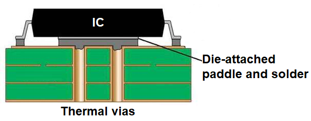
A thermal via does not have a particularly special structure; these vias are typically through-hole vias that can be filled with conductive epoxy and plated over. In this way, a thermal via will function as a heat pipe, aiding heat transfer away from a component on one of the surface layers and into the interior layers. The annular rings on a thermal via should poke through the solder mask and make contact with the die-attached paddle using solder. The vias are usually covered with solder mask on the back side of the board to prevent solder from wicking through the vias.

Thermal via design for heat transfer into the circuit board substrate
Thermal vias are will not be effective if placed far away from a component. Each via has higher thermal conductivity than FR4, so placing more vias will decrease the thermal resistance of the structure and will transfer more heat. In addition, each via has some inductance, but placing these vias in parallel and connecting them to the ground plane provides a lower inductance return path if the conductor on the bottom of an active component can be grounded. In general, you should opt for more vias if your manufacturing budget will allow up to the limits specified by the manufacturer of your components.
- Thermal vias should just be part of a larger thermal management strategy for your PCB.Learn more about creating a comprehensive thermal management strategy.
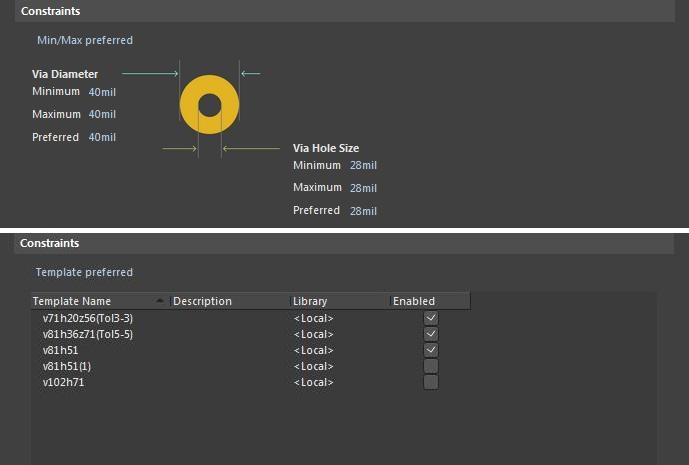
- When you place thermal vias in your board to aid heat transfer, you should check your placement against your design rules and constraints.
Learn more about design rule checking tools in your PCB design software.
- If you need to include thermal vias in your PCB, then you should carefully consider the PCB manufacturing process and adapt your design to ensure manufacturability.

Thermal via design and constraint editing in Altium Designer
Sizing Thermal Vias for Maximizing Heat Transfer
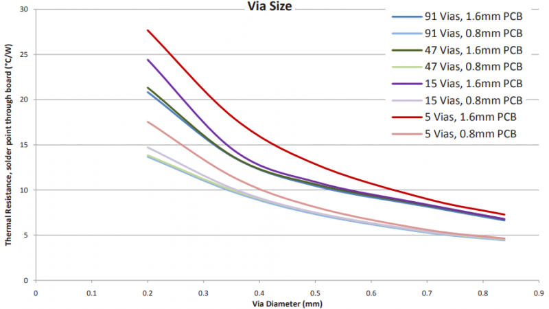
While it is difficult to make specific recommendations on thermal via sizes without conducting a thermal simulation, one can make some general statements regarding the placement and size of thermal vias in a circuit board. In addition to opting for more thermal vias where available, you should opt to use longer vias for a given via diameter. This will help minimize thermal resistance of your substrate.
For a given via length, you should opt to use wider vias, although this will limit the number of vias you can use with a given component. The graph below shows a summary of these design guidelines and their effect on thermal resistance in an FR4 substrate.

Thermal resistance versus thermal via length and number of thermal vias. Source: CREE.
Other Thermal Management Methods
In addition to thermal vias, there are other thermal management methods you can use to help bring the temperature of your circuit board and your components closer to ambient temperature during operation. Most laypeople are familiar with cooling fans used in computer CPUs, but these fans are effective for cooling active components through convection. When combined with a heat sink, thermal pad or paste, and thermal vias on high power components, you can easily keep the temperature of a component within its specified operating temperature.
Your PCB substrate and stackup determine can also aid thermal management and heat transfer throughout your board. The high thermal conductivity of copper planes in the interior layers of your circuit board aids heat transfer away from active components laterally, helping to produce a more even temperature distribution in your PCB. Note that placing a thermal relief to hold solder during manufacturing can have a negative effect on thermal management and heat transfer.
- Adding other passive heat dissipation techniques can help ensure your thermal management strategy keeps your board’s temperature as close to ambient temperature as possible.
Learn more about passive thermal dissipation techniques for your circuit board.
- There are many alternative substrate materials you can use to aid heat transfer away from active components, which will help decrease junction temperature and component temperature.
Learn more about working with alternative substrate materials.
- Working with thermal vias and other passive heat dissipation techniques can help you comply with IPC 2152 standards on thermal performance. Learn more about designing to IPC 2152 guidelines.

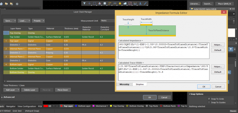
Your substrate material and your stackup will determine thermal resistance and heat transfer throughout your board
Software for Thermal Via Management
The best thermal via management software will include a powerful CAD interface and a complete set of via design tools for your circuit board. The best technology for managing thermal vias also includes stackup design and management features. This allows you to size and place thermal vias, as well as direct heat transfer to specific board layers and to help bring your board closer to ambient temperature during operation.
Integrated Thermal Via and Stackup Design in Altium Designer
Altium Designer’s complete set of CAD tools and routing tools are ideal for via design, including thermal via design and management. This allows you to easily route important signals throughout your layer stack and take advantage of thermal vias between specific layers.
- Altium Designer’s integrated design environment provides the important thermal via design and management features you need alongside other important conductor design tools. All these tools are integrated in a single design interface on top of a single rules-driven design engine.Learn more about unified design in Altium Designer.
- You can define important manufacturability constraints and industry standards as design rules thanks to the rules-driven PCB design engine in Altium Designer. This will help ensure your thermal via designs are fully manufacturable and will function as desired. Learn more about the rules-driven design engine in Altium Designer.
- Altium Designer’s materials stackup library allows you to choose from a large set standard substrate materials as part of a comprehensive thermal management strategy. Learn more about the materials stackup library in Altium Designer.
The CAD and thermal via design features in Altium Designer are ideal for easily placing important components, creating thermal vias to support heat transfer from these components, and defining your via manufacturing requirements as design rules. You’ll also have a powerful set of simulation features, and all available in a single program. Taken with the material stackup library and extensive component library, you have the tools you need to design a comprehensive thermal management strategy in a single design platform.
Altium gives you a huge set of resources for printed circuit design and has set a new standard in circuit board design and analysis. You’ll have access to the AltiumLive forum, podcasts and webinars with industry experts, an extensive knowledge base with plenty of design tips, and design tutorials. No other PCB design software company gives you this level of support. Instead of working with a fragmented PCB design platform, it’s time to take an integrated approach to design and management; it’s time to make the switch to Altium Designer.
