How to Design a Hybrid PCB Stackup

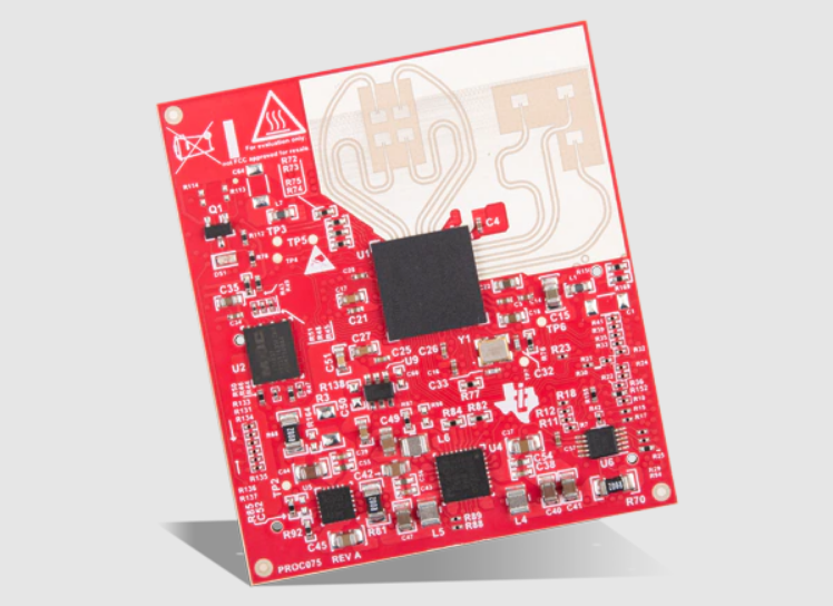
The radar evaluation module from Texas Instruments shown above is one example of a great way to design a PCB that contains an mmWave section complete with RF routing and high power transmission, as well as a moderate speed digital section with multiple ICs. I’m not affiliated with TI, but the main reason I like this board as an educational tool is that it shows one way to use PTFE-based laminates like Rogers or Taconic to build a commercial RF product. Sometimes, when we talk about using PTFE laminates or alternatives like low-Dk glass cloth laminates, we’re not talking about building the entire stackup from an expensive PTFE material with bondplies, or from low-loss materials like Megtron.
In some cases, it makes sense to build a board entirely from PTFE laminates or a low-Dk laminate. I’ve done this with high-speed backplanes that support dozens of long interconnects on multiple layers with bandwidth cutoffs at ~80 GHz. When you need to route multi-gig serial channels between two connectors across 15 inches of board space, you need to get losses as low as possible to ensure the signals at the receiver can be recovered. However, in other cases you really only need a low-loss laminate on one layer. This is the essence of a hybrid PCB stackup, and it may be a better choice for your board.
When to Use a Hybrid PCB Stackup
The first question that should come up when selecting materials and planning a stackup is: what materials are needed and how many layers should be used? Assuming you’ve determined you need a low-loss laminate and you’ve determined your required layer count, it’s time to consider whether you should use a hybrid stackup. There are a few broad situations where you could consider using a hybrid stackup with low-loss laminates in your PCB:
- Cost savings: Going all-PTFE or all-low-Dk can be expensive. For prototypes, the cost difference is not huge, but those cost differences add up at high volume.
- Low RF interconnect count: If you can fit all the high-speed/RF signals on one layer, it doesn’t make sense to build the entire stackup from specialized low-loss laminates. You might consider increasing the board size in order to reduce via count and fit everything on the low-loss layer.
- mmWave designs: Some RF systems operating in the ISM band or 6-7 GHz WiFi will operate just fine on FR4-grade laminates as long as interconnects are short. Once you get to car radar frequencies or higher, you will generally need low-loss laminates unless your interconnects are very short as to be impractical.
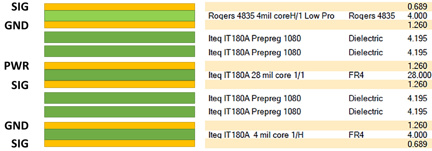
The image below shows a 6-layer hybrid stackup I presented in a previous post. This stackup is a good example stackup for radar modules or other specialty applications of mmWave signals like imaging.

The above stackup is also good for digital systems with bandwidths extending well into the mmWave regime, although watch out for dispersion in the low-loss laminate layer. RF material manufacturers try to build their laminate systems with flat dispersion out to high GHz frequencies. However, above some high frequency limit, dispersion will occur again to create more losses and phase distortion in digital signals. If you’re operating at extremely high frequencies above the dispersion-less limit, make sure to contact the laminate supplier for dielectric constant data so you can run accurate impedance and S-parameter calculations.
In addition, some fabricators might tell you this stackup can’t be manufactured because you’ve placed PWR and SIG adjacent in the two internal layers. If the board is small, it won’t matter; this board won’t experience any bowing until its span reaches multi-U backplane sizes. You can also balance the internal layer with copper pour if needed.
Talk to Your Fabricator Early
If you’ve put together a hybrid stackup based on your loss requirements, circuit board thickness, and layer count, you should send your stackup to your fabricator before you start your design. This is quite important as your fabricator can determine if the board will pass through the lamination cycle without decomposing or undergoing delamination as some materials need higher temperatures and pressures than others. Don’t be afraid to contact a fabricator early for their advice on using your desired low-loss laminate in a hybrid stackup. Be sure to give them:
- Required layer count
- Desired layer thicknesses
- Cap low-loss laminate material
- Filler laminate materials
Try to decide which requirements are must-haves vs. nice-to-haves as you might need to compromise on some of your requirements.
Allow Room for Bondply
Your fabricator can give you some insight into the thickness variation you can expect to see in the finished board once bondply is added. Make sure to consider this when planning the stackup. You generally do not need to worry about the dielectric constant of the bondply layer unless you need to route over it. If you’ve designed with a low-loss laminate on the top layer, the bondply may need to sit between L2 and L3 so that the low-loss material adheres to the FR4-grade laminates. Your fabricator can give you more information on this point.
Submit a Preliminary Stackup
Even after you create a preliminary stackup, you should send it in to your fabricator so that they can inspect it before fabrication. Sometimes, you aren’t free to choose just any material system and low-loss laminate you want to use in a hybrid stackup. Your fabricator will have a say in which materials are available, have low lead time, or if they will have to outsource fabrication. If you can get your stackup reviewed before you create the rest of your design, your fabricator could recommend an alternative material system that is compatible with the required PCB lamination process. They may also recommend some alternative laminate thicknesses that can help you reach your overall circuit board thickness requirements.
Reading Material Datasheets
If you’re selecting materials for a hybrid stackup and you want to take a more active role in building a hybrid stackup, take a look at the datasheets for the materials before you create a proposed stackup. Try to match CTE values, Tg values, and resin flow temperature, and cure temperature to ensure full compatibility. You should still send in the stackup for review to ensure manufacturability.
When you need to create a hybrid PCB stackup, the PCB design tools in Altium Designer® include everything you need to specify your stackup construction, calculate impedance, and import the stackup information into fabrication drawings. The Draftsman utility helps you quickly create fabrication and assembly drawings with your hybrid PCB stackup and export them in PDF format. When you’ve finished your design, and you want to release files to your manufacturer, the Altium 365™ platform makes it easy to collaborate and share your projects.
We have only scratched the surface of what’s possible with Altium Designer on Altium 365. Start your free trial of Altium Designer + Altium 365 today.
