How Antipads Affect Signal Integrity in Your Multilayer PCB
Antipads on vias and landing pads are a point of contention in modern PCB design, and the debate around the use of these elements in a multilayer PCB is framed as a binary choice. Like thermal reliefs, ground plane splits, and orthogonal routing, the debate around antipads on landing pads and vias is framed as an always/never choice. With today’s modern PCBs, it pays to understand the effects of antipads on signal integrity.
Antipads and Signal Integrity
When it comes to signal integrity, be careful with application notes from component manufacturers, and always validate what you see from well-understood concepts. If you look at some component application notes, they will recommend placing antipads on landing pads without explanation. In addition, different notes will tell you precisely the via antipad diameter you should use, but it is easy to take this out of context. Let’s look closely at these two situations and how the structure of a via/pad + antipad can lead to signal integrity problems.
How to Model a Via and its Antipads
A via antipad is applied automatically by your CAD tools based on your clearance rules anytime you use a plated-through hole to transition through a solid plane. If you’re routing through a plane layer, your options are to completely remove a large section of the plane around the via or encircle the via in the remaining conductor to create an antipad. No matter what happens, there must be some void between the via wall and any planes in order to prevent shorting.
At this point, if you’re routing through a solid plane, the question is not whether you should use a via antipad or cut away the plane around the, but rather how large should the antipad extend past the via pad and any internal nonfunctional pads. Like many potential problems in high speed design, all vias have parasitics:
- Inductance. A via taken in isolation is basically an inductor, and the inductance of the via depends on the via aspect ratio.
- Capacitance. The presence of the plane around creates some parasitic capacitance between the via pads and ground.
Each pad at the end of the via and the intervening plane creates two capacitances in parallel. When combined with an inductor, we have a standard pi model describing a via and their antipad, as shown below. Note that the capacitance equation shown below is only an approximation as it does not consider fringing fields. The via inductance equation is also an approximation.
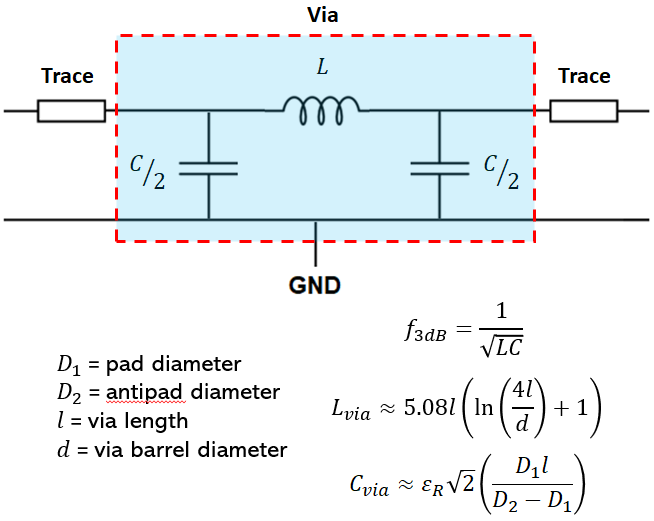
What happens next (in terms of electrical behavior) depends on a number of factors. First, just like any pi circuit, the CLC pi model is basically a low-pass filter with the 3 dB cutoff frequency defined above. Suppose you want to extend the bandwidth of your via + antipad arrangement. In that case, you’ll need to reduce the aspect ratio (shorter via or wider barrel diameter), or decrease the pad-plane-pad capacitance (larger antipad).
Here, you have a difficult set of options to balance. Modern designs are getting denser with smaller features, so there is a danger your aspect ratio becomes quite large, the 3 dB frequency would decrease and limit bandwidth. Once you get to the mmWave regime, you’ll have other signal integrity challenges involving routing through vias. Additional parasitics become dominant at these frequencies and contribute to overall insertion loss along an interconnect.
How an Antipad on a Landing Pad Affects Signals
Placing an antipad on a landing pad involves cutting away some ground plane beneath a pad on a component. An example on an antenna feedline is shown below (pad + antipad is circled in yellow). The antipad in the blue ground plane region is shown below and was placed as a polygon cutout.
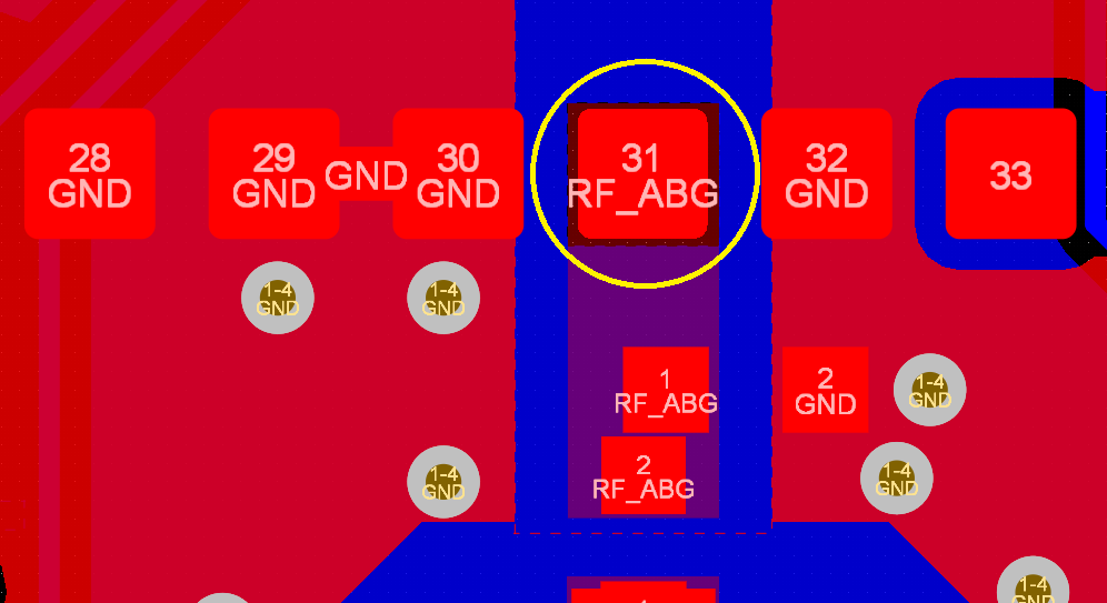
There is one good reason to do this, but there are other reasons you should not do this, and they outweigh each other at different frequencies and in certain situations. In the above case, placing the antipad eliminates some parasitic capacitance; the field carried by a signal then couples back to the ground plane only through fringing fields. This is one alternative to using a smaller landing pad.
The above example is a bit contrived, and I would not do this in a customer’s board without validation through simulations, but it illustrates a good point about return path planning. Even though there is a ground cutout below the pad, there is still a clear return path through nearby vias and ground pour, so a major impedance discontinuity is not created in this process. Without such assistance from ground pour and vias back to a reference plane, you’d create a significant impedance discontinuity due to a large return path.
Summary
In summary, if you want to control via bandwidth and parasitics, you have a few levers you can pull. Antipads on vias give you a simple way to tune the parasitic capacitance to match the inductance for a given via aspect ratio. The dielectric constant (Dk value only) can also be used as a tool for controlling via capacitance.
Regarding antipads on landing pads, you’ll create a small impedance discontinuity, which can create some small insertion loss and return loss at the pad. In high speed channels where bandwidths can extend up to 100 GHz and beyond, every last bit of insertion loss you can avoid is critical. My view is to play it safe and not use any antipads on landing pads unless you absolutely need to do this to set a landing pad’s impedance to some specific value, thereby reducing return loss.
Whenever you need to design an antipad for use in your PCB, you can use the complete set of rules-driven design tools in Altium Designer®. When you need to share your work with your collaborators, you can use the Altium 365® platform to share and manage your design data. We have only scratched the surface of what is possible to do with Altium Designer on Altium 365. You can check the product page for a more in-depth feature description or one of the On-Demand Webinars.
