CAN-Bus: Designing CAN-Bus Circuitry
This article is part of a three-part introductory series on the CAN-bus:
- Part 1: An Informal Introduction
- Part 2: The Protocol
- Part 3: Designing CAN-Bus Circuitry
Introduction
There are three main components in a CAN-bus node:
- Microprocessor
- CAN-bus controller
- CAN-bus transceiver
The CAN-bus controller implements all the low-level features of the network protocol, ISO 11898–1, while the transceiver communicates with the physical layer. Different transceivers are required for different physical layers, such as high-speed can, low-speed fault-tolerant can, or high-speed can with variable data rate.
In a typical implementation, the CAN-bus controller and microprocessor are unified into a CAN-enabled microcontroller. External CAN-bus controllers with SPI interface are available on the market, mainly manufactured by Microchip, but they often can add unnecessary cost and complexity.
In this article, we’ll take a look at circuit design from the transceiver to the can-bus connector. It’s time to get our hands dirty and design our CAN-bus circuitry!
Step One - Choose the Right IC
All CAN-bus transceivers operate similarly, as they sit between the microcontroller (or FPGA) implementing the CAN-bus controller and the CAN-bus itself. Still, there are a few differences that you should consider carefully.
A quick search on the appropriate Octopart category reveals the leading manufacturers of CAN-bus transceivers are, in descending order by the amount of ICs offered, NXP Semiconductors, Microchip, Texas Instruments, Maxim Integrated, Analog Devices and ST Microelectronics.
All these transceivers look alike, yet they all differ in their features and performance.
ESD Protection
The first CAN-bus transceivers on the market included very little protection from ESD (Electro Static Discharge) events. They required all the I/O protection to be implemented with external components.
Luckily, this is not the case anymore. Here are a few random ICs and their HBU (Human Body Model) ESD tolerance on the bus pins:
|
Part Number |
Manufacturer |
ESD HBM Tolerance |
|
L9616 |
ST Microelectronics |
6kV |
|
IFX1050G |
Infineon |
6kV |
|
TJA1051 |
NXP Semiconductor |
8kV |
|
LTC2875 |
Linear Technology |
25kV |
|
MAX14883E |
Maxim Integrated |
22kV |
Higher ESD tolerance may allow you to save on external protection, but you should be aware that a few extra cents spent on quality TVS diodes can dramatically improve reliability.
If your application is space-constrained and you don’t have to deal with much ESD, then all-in-one is the way to go. In my case, I went with an external TVS and a more affordable transceiver.
Operating Voltage
Most transceivers on the market operate at 5V, but ICs designed for 3.3V are extremely popular as well. Lower supply voltages are not possible without recurring to the use of dc-dc converters. Some ICs, such as Maxim Integrated’s MAX14883E include a logic-level supply input enabling interoperability with 1.8V devices regardless of the transceiver’s supply.
.png)
In my case, my MCU operates at 3.3V, so I’ll choose it as well for the CAN-bus transceivers.
Speed
All High-speed CAN-bus transceivers can operate up to 1Mbps on small networks. CAN-FD transceivers can be operated at up to 5Mbps, but many of them are limited to lower speeds such as 2Mbps.
The final system data-rate will be limited by the bus capacitance, the allocation of CAN-bus identifiers, and the type of CAN frames being transmitted. Worst case scenario is usually an effective baud rate of one third the maximum.
Isolation
An isolated CAN-bus transceiver may be needed either for safety requirements. For example, introducing galvanic isolation can protect the low-voltage part of your circuits in case the bus enters in contact with dangerous voltages. The same isolation can also improve communication by breaking up ground loops and allowing more substantial differences in ground potential between nodes.
Of course, isolated CAN-bus transceivers will require a similarly isolated power supply.
Power-Saving Features
Many transceivers include a mode-select input that can be used to put the IC low power consumption and switch off the transmitter. Typically, the receiver remains active, and the RXD pin can be used to trigger a wake-up interrupt in the microcontroller.
The mode select input sometimes doubles as slope-control when it’s pulled high or low through a resistor of at least a few kOhm. Reducing the signal slope, while it can limit the bandwidth, allows the transceiver to restrict the amount of electromagnetic interference it produces.
Bus and Common-Mode Voltage Range
All ISO 11898–2 compliant transceiver must be able to withstand DC voltages on CANH and CANL between -3V and +32V to ground without breaking, withstand transients of -150V to 100V, and be able to operate with a common-mode bus voltage between -2V and +7V.
Virtually all ICs on the market exceed these requirements, with an informal contest of who can show off the most significant numbers going on in the background.
Here are a few examples:
|
Part Number |
Manufacturer |
DC voltage on CANH and CANL |
|
L9616 |
ST Microelectronics |
-5V to +36V |
|
IFX1050G |
Infineon |
-40V to +40V |
|
TJA1051 |
NXP Semiconductor |
-58V to +58V |
|
LTC2875 |
Linear Technology |
+60V to +60V |
|
MAX14883E |
Maxim Integrated |
+63V to +63V |
Voltages above 50V are now standard, as many vehicles feature hybrid powertrains operating at 48V, and the transceiver should be able to withstand a bus short to the higher-voltage supply rail of the system.
Input Impedance
There are no hard and fast rules on how many nodes you can fit on a network, but one of the most critical parameters will be the input impedance between CANH and CANL on your transceiver.
A high input impedance will have a marginal influence on the bus and enable a higher number of nodes.
Smart Protection
Some transceiver implements extensive protection features, such as:
- Dominant state time-out: if the bus stays dominant for too long, for example, due to a hardware or software failure, the output driver is disabled.
- Thermal shutdown.
- Undervoltage lockout: the device is disabled in under-voltage conditions.
- Recessive underpowered state: when not powered correctly, the device does not drive the bus in any way.
- Current-limiting: protection in case of short to either positive or negative supply voltage.
Autobaud and Listen-Only
Most CAN-bus transceivers include a listen-only mode that feeds back the TXD to the RXD without actually driving the bus. This feature is often used to determine the bus baud rate automatically.
My Choice
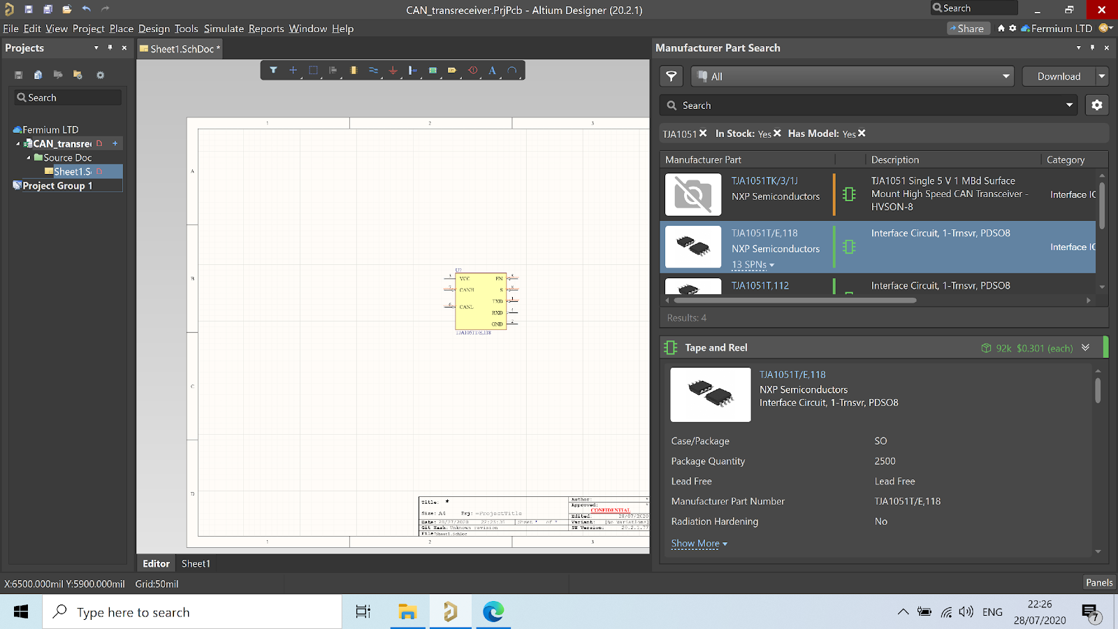
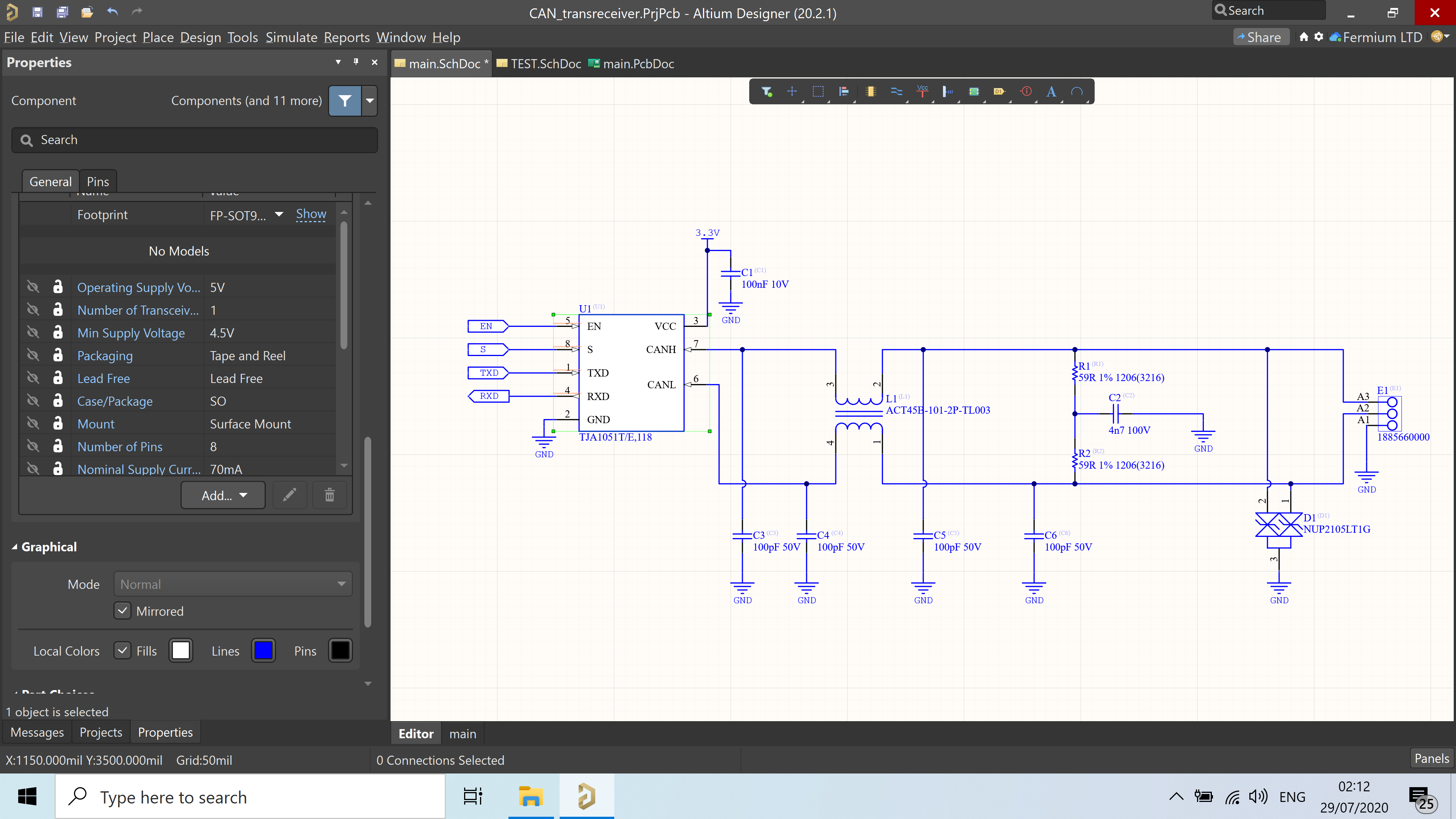
In my design, I went with a TJA1051, mainly because I’m cheap, and it’s one of the most affordable ICs on the market. The product page can be found here.
Using the “Manufacturer Part Search” panel, I immediately found the component models, complete with footprint and 3D, and placed them on the schematic. The model was automatically downloaded from Altium 365®’s cloud libraries.
Step Two - Corollary Passives
Filtering
I don’t need to mention we’ll need local bypass capacitors, do I?
Additionally, some extra small-values capacitors of typically 40 to 100pF on the CANH and CANL lines and connected to the ground can help absorb ESD energy and improve EMI resilience. As always, with increased bus capacitance comes decreased bus speed, increase loading of the transceiver output stage, and increased power consumption.
Termination
The CAN-bus should be terminated at each ends with a 120-ohm resistor. Of course, we could properly calculate the wattage (1/4W standard, 1/2W if we’re paranoid), place our cute little resistor and call it a day. But why make things simple?
A more sophisticated technique, adopted in almost all industry-proven CAN-bus boards I’ve seen so far, is split termination.
In split termination, two 60 ohm resistors are used in series, totalling 120 ohms. The electrical node between the two resistors is connected to ground through a capacitor, usually of 4.7nF.
The value of the capacitor has been calculated to obtain a -3db cut-off frequency at the fundamental frequency of the network.

In my case, the network should have a 1mbit/s baud rate. Assuming the worst-case scenario, when the network is transmitting a sequence of alternating bits (01010101) the signal will be a square wave of frequency 500kHz, or equal to half the baud rate.
We know the resistance at 60 ohms, we can thus calculate the capacitor.

If we have to approximate our capacitor’s value, a slightly smaller one will interfere less with our precious signal. Hence, 4.7nF, which is the most broadly adopted value.
If you need a library of passive components, I wholeheartedly recommend Mark Harris’ Celestial Library. It’s free, extensive, and carefully curated.
TVS
If your system is not subject to heavy ESD, the included protection in the transceiver IC could be everything that is needed.
TVS (Transient Voltage Suppressor) diodes are a common choice due to their low equivalent parallel capacitance.
Other over-voltage protection devices, such as MOVs, often have a high parasitic capacitance that can limit the bus data rates, especially for busses with many nodes.
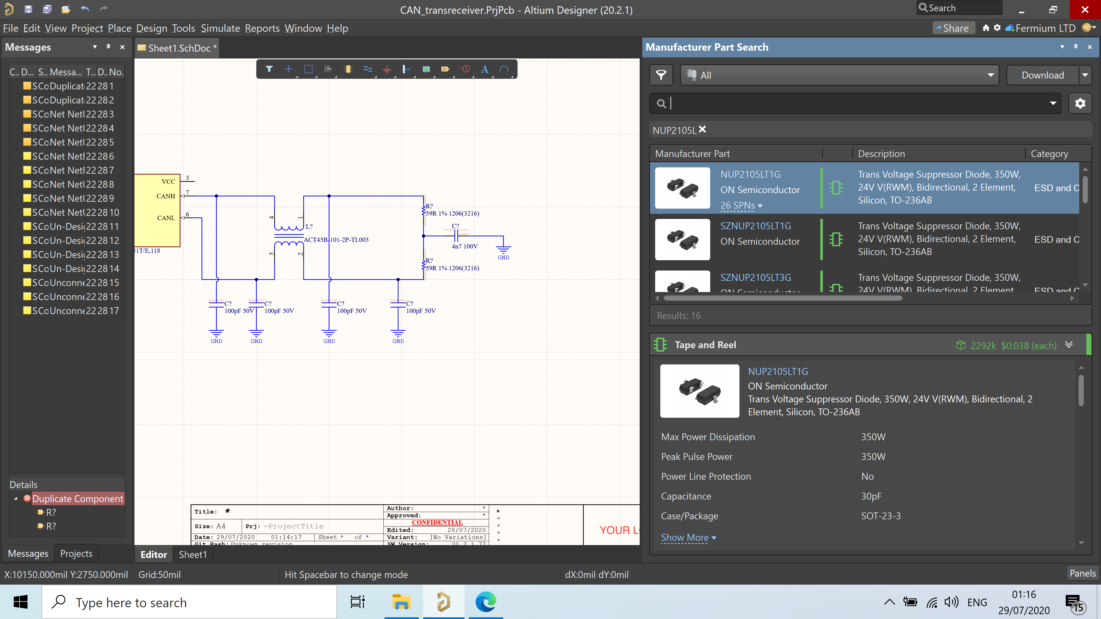
Several TVS diodes specially designed for CAN-bus are available on the market, for example, NUP2105L by ON Semiconductor, which I have decided to employ in this design.
As for the transceiver, I placed the model with one click from Altium 365 libraries using the Manufacturer Part Search panel, without having to draw the schematic symbol and footprint.
Step Three - Design the PCB
Keep it tight (unlike this article)
If your circuit were without protection, all the EMI current would go straight into your transceiver from your connector, and then back through the ground plane. That’s what the current wants to do because that’s the path of least impedance.
All your protection components should be as close as possible to that path to avoid increasing the loop area. Additionally, all the protection should be as close as possible to the connector and the board’s edge to prevent noise coupling into the rest of the circuitry.
Naturally, it’s not possible to cram everything in direct proximity to the connector, so we must prioritize. The general rule of thumb is to place the component that has to deal with the “worst” EMI offender first.
In our case, TVS diodes have to deal with high-speed high-current events. As fast impulses are rich in high-frequency components, if left unchecked to roam into our boards, they will couple with every available trace and disrupt operation.
So the TVS goes first.
If we didn’t have the termination resistors in the middle, the common-mode choke would go second.
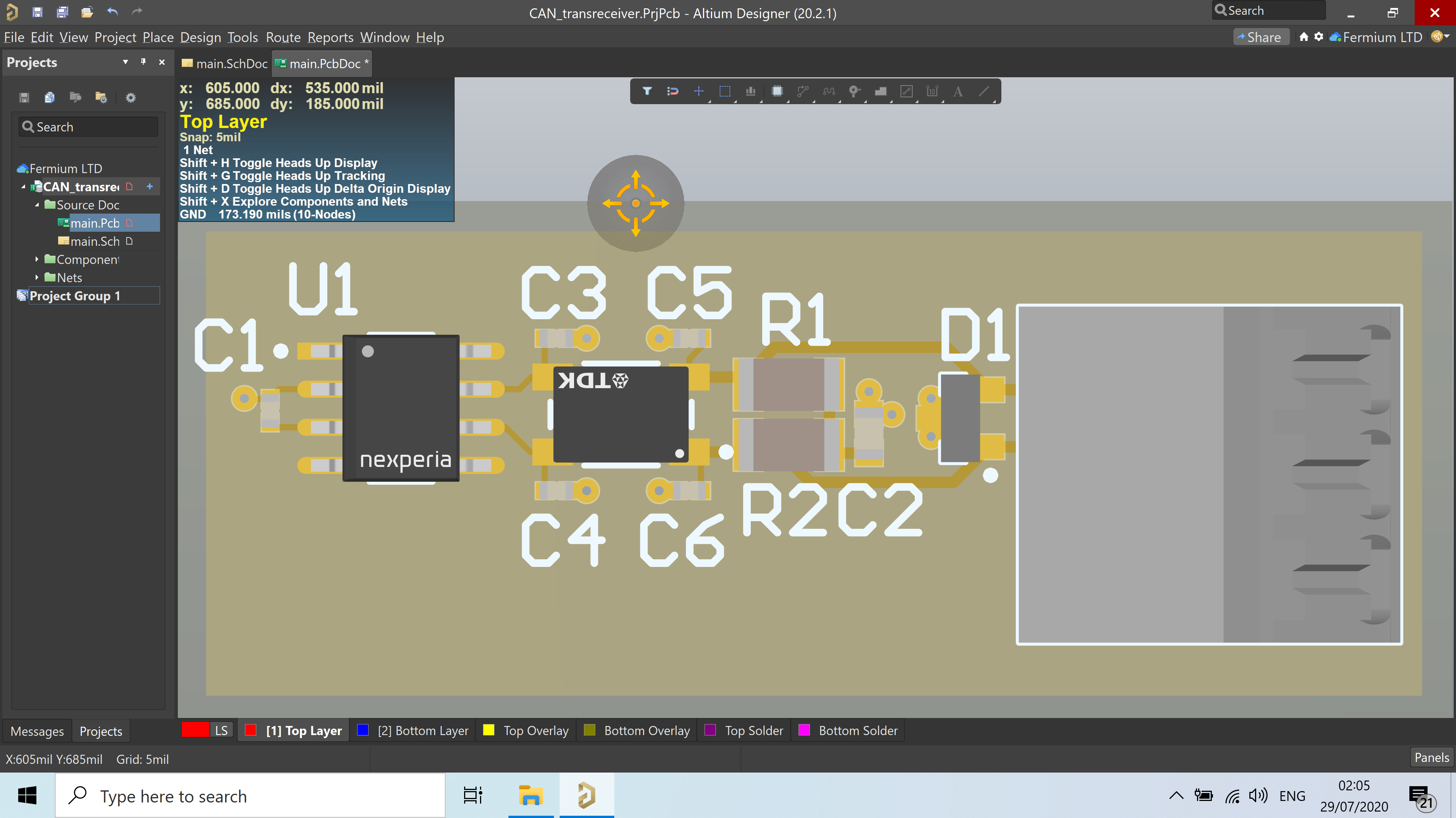
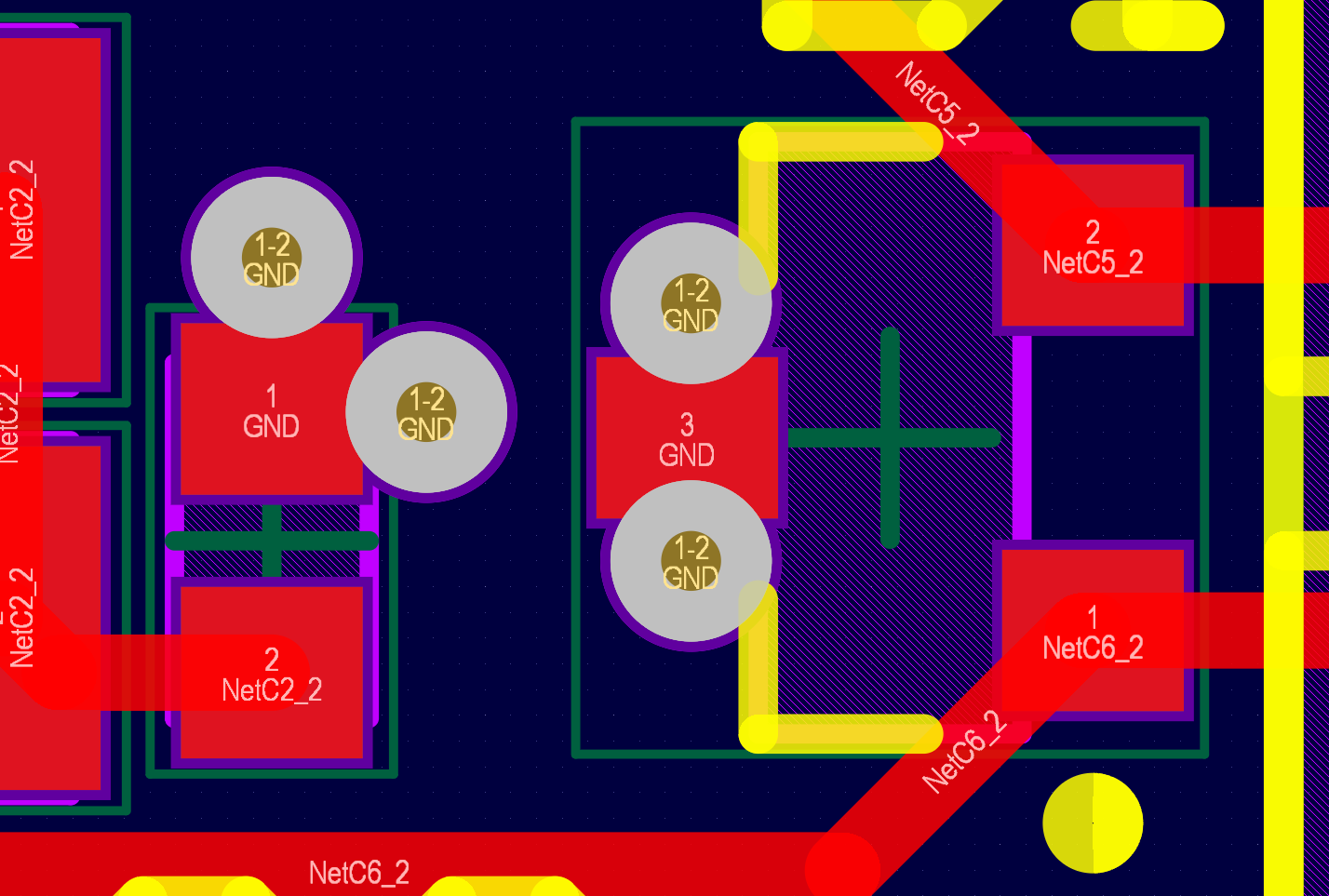
In our example PCB, there is still room for improvement. The TVS diode could be rotated by 180 degrees to reduce the ESD loop area further. The capacitors C5 and C6 could be rotated 180 degrees as well and moved a tiny bit to the right.
Use the Planes
Every PCB layout guide has written in it “ground planes this” or “ground planes that”, and if you want to keep that EMI far away from the supple belly of your boards, there is no escaping it.
Use ground planes.
There must be a ground plane right underneath whatever signal you’re clamping to ground to keep the path of least impedance as short as possible. Your TVS diodes should discharge the impulses directly to the ground plane, connected to the cable shield (if available) through a low-inductance connection.
Use Low-Impedance Via Techniques
It doesn’t make much sense to spend all our hard-earned pennies on capacitors if their effect is going to be nullified by the inductance of the ground traces.
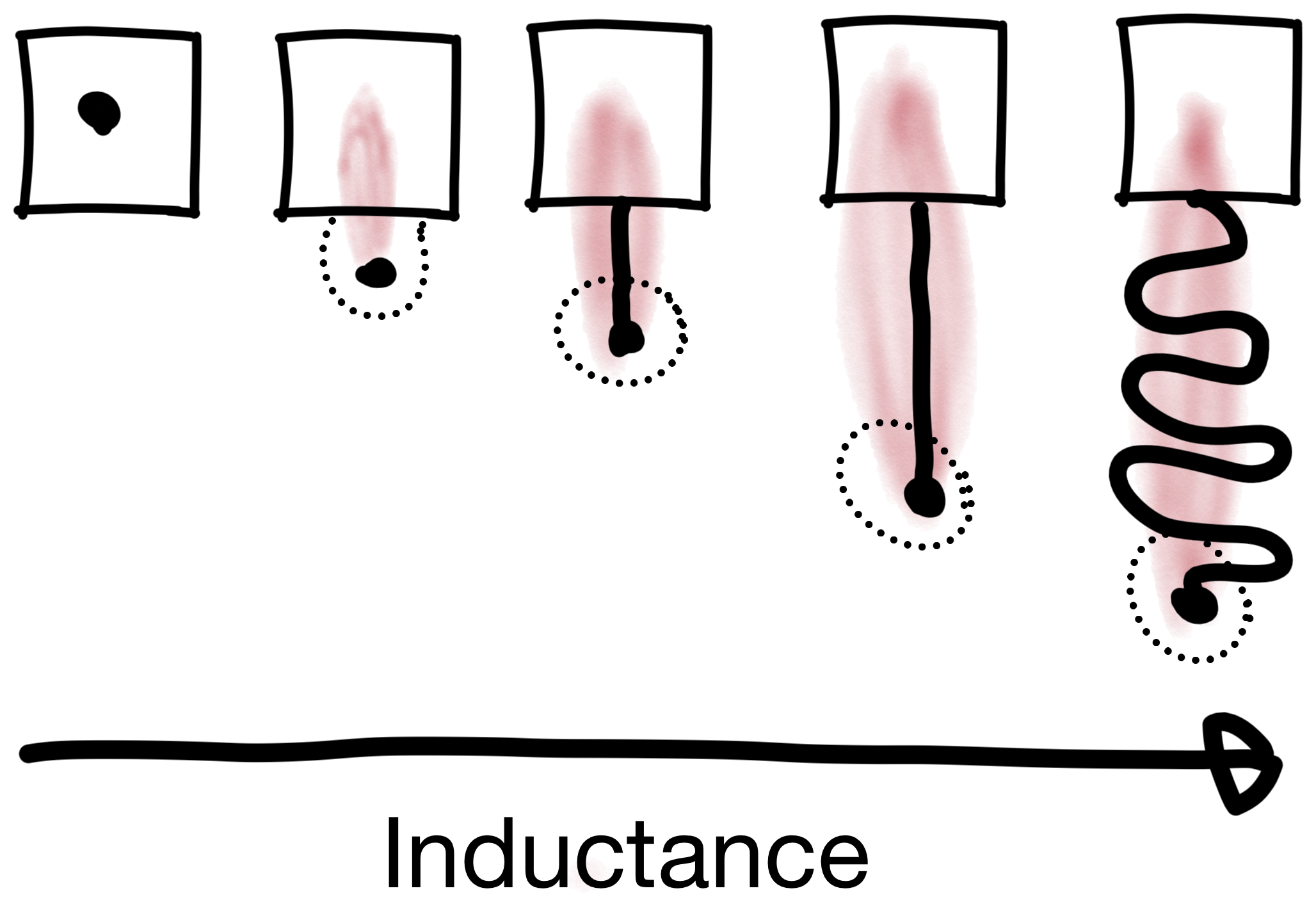
In this design, I’ve used vias on the outskirt of the pad. Unlike the via-in-pad technique, it doesn’t require an extra step in the manufacturing of the PCB and thus does not increase the cost. The via must be tented; otherwise, the solder paste will flow inside, and the pad would not be adequately wetted.
You can find documentation on Altium Designer via properties here.
Step Five - Sharing (The Unadulterated Sales Pitch)
Let’s say we’ve now spent hours reading articles written by dubious figures, researching transceivers, testing and validating our perfect CAN-bus subcircuit. Now what?
With Altium Concord Pro™, you can share your schematic sheets with your whole organization, and it only takes a few seconds.
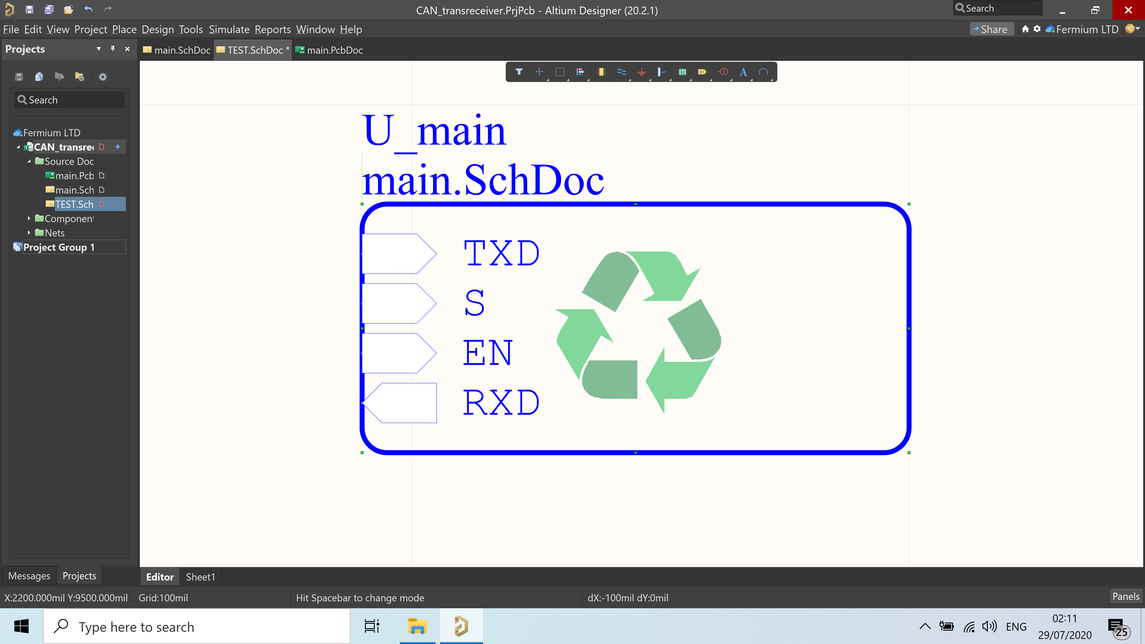
The first step is designing your circuit in a single schematic document, using ports for input and outputs, similarly to what you would do for hierarchical design.
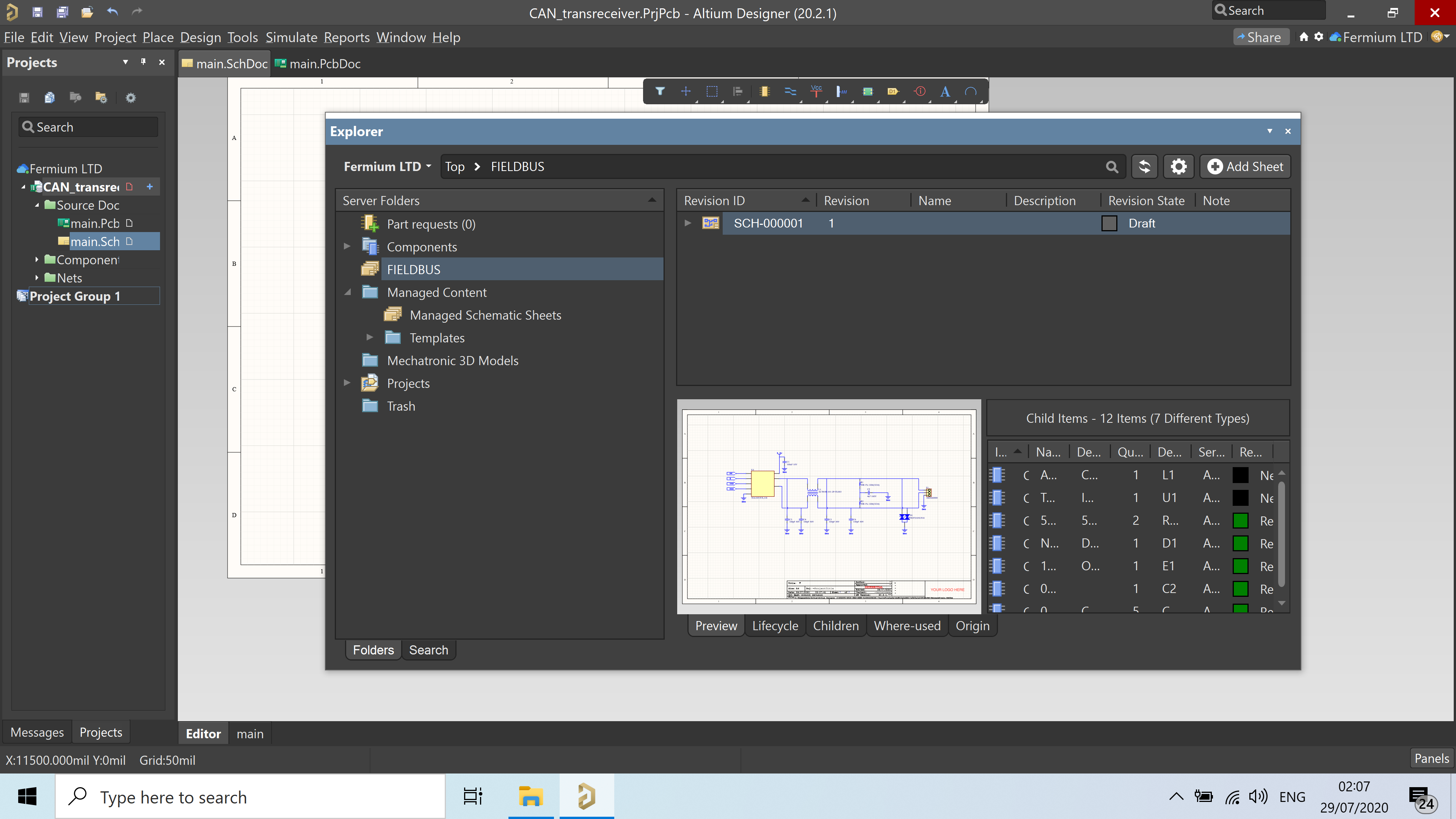
Using the explorer panel, create a new “Managed Schematic Sheets” folder.
.png)
Once your folder has been created, all users within your organization will have access to it, and you can proceed to upload the schematic sheet.
You can now place your managed schematic sheet in any project.
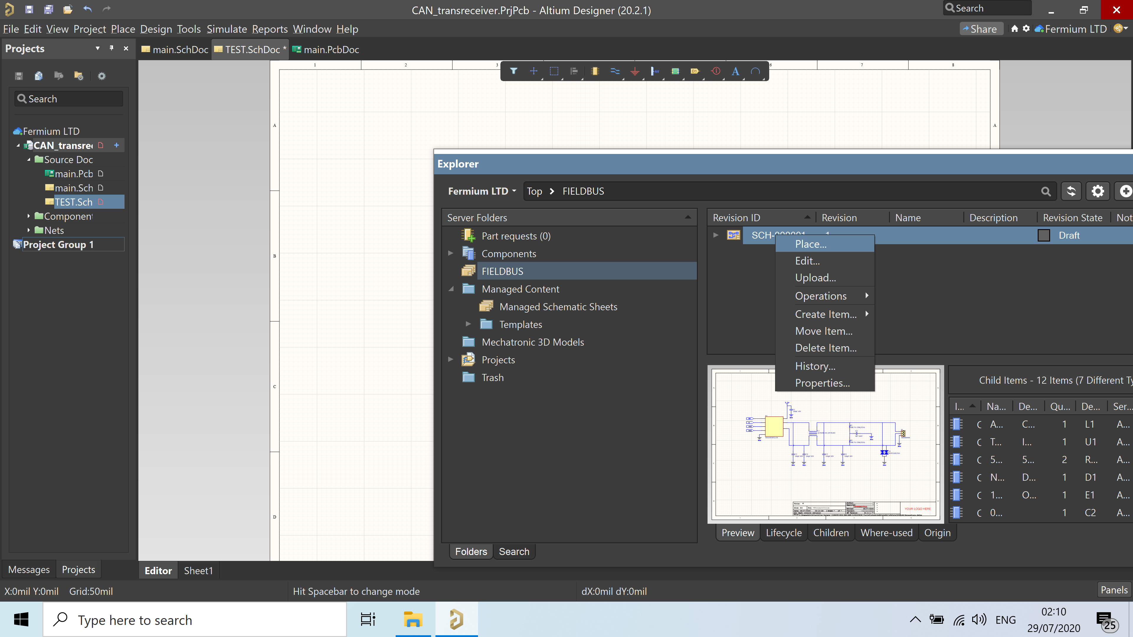
Your new managed schematic sheet will be differentiated by the “reuse” green symbol.
If you’d like to know why everything is blue instead of yellow and red, check my previous article about design styling.
Tips and Tricks
Add extra termination for the stubs
An optional “weak” termination, for example, 1.3Kohm, can help improve the EMI resilience of nodes with a long stub distance. The same resistance, however, contributes to load the network, reducing the number of nodes, decreasing the final nominal impedance of the bus, and reducing the maximum speed.
More is better. Or not?
If you’re not cost-constrained and input protection is paramount to you, you should consider adding a second round of protection:
A MOV (Metal Oxide Varistor) or GDT (Gas Discharge Tube) to “absorb” higher energy than what the TVS can handle.
Some current-limiting device between the MOV/GDT and the transceiver, such as a high-impulse resistor, a varistor, or a TBU® (a fancy semiconductor varistor sold by Bourns).
It would help if you always kept in mind, however, that these devices may increase your equivalent bus capacitance and lower your data-rates and increase current consumption.
Common-mode chokes are amazing, but dangerous
Standard mode chokes are the most common type of filter used on CAN-Bus, and they work great, but they have some drawbacks you should consider.
Common-mode chokes can create resonances with the parasitic capacitance of the CAN-bus bus, leading to increased noise in a few specific frequency bands. This effect can make the EMI properties of CAN-bus devices unpredictable, since the inductance in common-mode chokes is rarely specified precisely, and the parasitic capacitance can vary wildly with cable lengths. If an unshielded cable is used, the capacitance can vary depending on the proximity of the cable to grounded metal surfaces.
As we all know, common-mode inductors behave as inductors in common mode. Duh. Some fault conditions, such as a short to power or ground, can cause high transient common-mode currents. In some cases, the overvoltage created by the inductance of the common mode choke can damage the CAN-bus transceivers. These over-voltages can be rather nasty to debug, as they are created after the overvoltage protection, which is typically placed at the edge of the board.
The third drawback of chokes… they can be expensive. High-speed differential signals require very low current leakage.
Some IC manufacturers, Texas Instruments, in particular, are pushing isolated and highly EMI-tolerant devices for “choke-less” CAN-bus networks.
I’m quite fond of them, so I decided to go with a common-mode choke specifically designed for CAN-bus applications.
Conclusion
I must be in love with the CAN-bus. Between its endless flexibility and the extreme EMI resistance, it’s, without doubt, one of the most exciting standards in the world.
With Altium Concord Pro you can seamlessly share your schematic sheets inside your organization, enabling design reuse and minimizing the engineering effort to launch new products.
Have more questions? Call an expert at Altium.