How to Select an Inductor for a Buck Converter
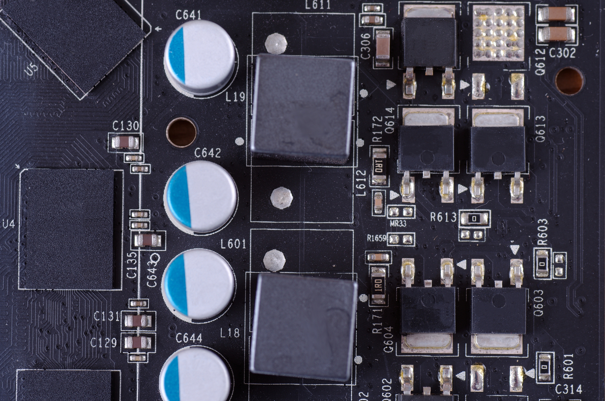
An SMPS is one of those quiet (yet electrically noisy) devices that makes your favorite electronics run smoothly. They sit in the background quietly doing their duty, yet your board wouldn’t operate without them. As part of DC-DC converter design for power-hungry applications, component selection is quite important for ensuring stable power delivery to a load with high efficiency.
Among the numerous DC-DC converter topologies, a buck converter finds plenty of uses for stepping down the input voltage to a lower level while providing high efficiency power conversion. A common question around component selection for these power converters is how to select an inductor for a buck converter. The goal in working with an inductor and other components in a buck converter is to limit power loss to heat and while minimizing current ripple.
Inductors in a Buck Converter
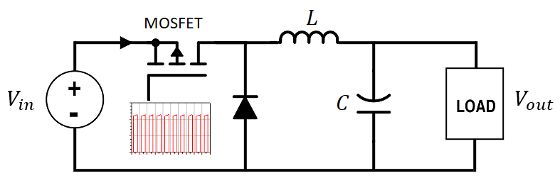
The basic buck converter topology for an SMPS is shown below. In this diagram, the output from the MOSFET is driven with a PWM signal, which turns the MOSFET on and off with a user-selected duty cycle. The inductor and capacitor play a critical role in providing stable current to the load as the PWM signal switches. Finally, the duty cycle of the PWM signal is the primary function allowing the user to control the output voltage delivered to the load.
The inductor will be constantly switching at the same rate as the PWM signal, thus it is responsible for superimposing some slight ripple on the current sent to the output. The inductor and the capacitor form an L-filter, which is basically a 2nd order bandpass filter. Assuming you use a sufficiently large capacitor with low ESR, the capacitor will provide low impedance and high frequency components making up ripple will be largely removed.
How to Select an Inductor for Your Buck Converter
The appropriate value for your inductor depends on the desired ripple current your design can tolerate, as well as the duty cycle you plan to use for your PWM signal. The following equation shows the output voltage as a function of the diode forward voltage drop and the ON-state voltage drop across the MOSFET. After accounting for these voltages, the output voltage is:

I’m going to skip some math and get straight to the important results. First, the inductance and PWM frequency are inversely proportional to the ripple voltage. Second, the ripple is also a quadratic function of the PWM duty cycle. The ripple current in the buck converter is:
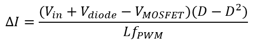
Note that the rise time of the PWM signal does not appear in either equation. However, the rise time is important in that it plays a role in determining the noise emitted from the converter and losses (see below for more details). The important results can be summarized as follows:
- Increasing the duty cycle will reduce ripple, but it will also bring the output voltage closer to the input.
- Increasing the PWM frequency will reduce ripple, but this will increase heat dissipation in the MOSFET. Again, there is a caveat to this: using a PWM signal with a faster edge rate will reduce these losses from a higher PWM frequency (again, see below).
- Using a larger input voltage requires using a larger inductor in order to reduce ripple to an acceptable level. In general, use a larger inductor to reduce ripple.
Why the PWM Rise Time is Important
The inductor is responsible for creating and simultaneously suppressing ripple on the output current, although this can be set as a design goal in the design using the above guidelines. However, there are some important aspects of any switching regulator that the inductor can’t control:
- Radiated EMI from the switching element: this switching noise from the transistor can induce some noise in downstream circuits.
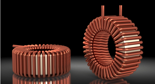
- Thermal losses due to the skin effect: this is a function of the geometry of the inductor and not the inductance value. If the inductor has a larger cross-sectional area and higher thermal conductivity, heat can be dissipated from the inductor at a higher rate.
- Thermal losses in the transistor: the transistor dissipates the lion’s share of heat during switching and regulation. However, using a faster edge rate will suppress this heat loss as the MOSFET will more fully switch off between PWM oscillations.
These sources of noise depend on the frequency and edge rate of the PWM signal. If you run a buck converter at a higher switching frequency without changing the duty cycle, you would normally lose more power as heat in the MOSFET. The tradeoff to using a faster edge rate is the risk of more high frequency noise induced in downstream circuits and more heat lost via the skin effect. Read more about these points in this article.
With the schematic design and PCB layout features in Altium Designer®, you can create the board you need for your next power supply and prepare your designs for manufacturing. You’ll also have access to a huge range of components, with schematic symbols and 3D models provided directly by manufacturers. All these features are accessible in a single design environment, which helps you remain productive and get your next product built quickly.
Now you can download a free trial of Altium Designer and learn more about the industry’s best layout, simulation, and production planning tools. Talk to an Altium expert today to learn more.
