Your Complete Guide to Via Stub Analysis
Via stubs are sometimes viewed as an annoyance, especially when you only need to make a transition between adjacent layers. For low speed, less-dense boards with low layer count, via stubs are an afterthought, or they may not receive consideration at all. For faster edge rates/higher frequencies, the conventional wisdom is to remove all via stubs. The question is: what exactly counts as “high frequency,” and how do you figure out the relevant length?
To do this correctly, you’ll need to borrow a few tools from circuit theory to understand the electrical function of a via stub, and you’ll need to borrow some elements from transmission line theory. As it turns out, just like a regular trace on a PCB, an electrically long via stub will act like a transmission line. It gets more interesting when we consider what happens at high-GHz frequencies in a real PCB, where parasitics become problematic. So to properly understand via stubs, we have to look at them from two perspectives: using a circuit model and as an electrically long structure with propagating waves.
Via Stub as a Circuit Model
I’ll be one of the first people to tell you that circuit models are not exact for describing real designs. Circuit models, especially RLC circuits, are very useful as a language that can describe electrical behavior, but circuit models should not be taken literally. That being said, we can still intuitively create a circuit model describing via stubs by looking at the structure of a via, any nearby conductors held at constant potential (power/ground planes), and the transmission line sections connected to it.
The image below shows a diagram of a typical via with its stub, nearby pads/planes, and some circuit elements to indicate the electrical behavior in different portions of the via/stub. The electrical behavior is dominated by the series inductance and resistance in the via and stub. However, there is also parasitic capacitance back to the other conductors, as shown with the capacitor symbols.
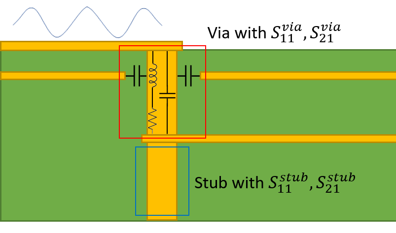
The electrical description of a via is normally as an inductor with some non-zero DC resistance in series (thus the series inductor and resistor symbols in the above diagram). This means the impedance of the via, including the skin effect and copper roughness, would be:

In this equation, the copper roughness factor K basically increases the skin effect resistance and has a complicated spectrum; research on properly modeling copper roughness continues to be active. Basically, the via’s impedance can be modeled as inductive at sufficiently low frequencies. This equation is only an approximation, however, as the via impedance is in parallel with a distributed capacitance back to nearby conductors. At high frequencies, the capacitive elements become much more important, which allows signals to “bleed” into the nearby conductors via capacitive coupling.
As we have distributed shunt capacitance with distributed series inductance and DC resistance, the real via impedance equation matches that of a transmission line! As such, the via and via stub create some insertion loss and return loss (defined with S-parameters) seen by the propagating signal. So now, to properly determine the appropriate stub length, we need to think about a via, the via stub, and the input/output lines as various transmission line sections.
Via Stubs as Transmission Line Sections
If you think about it briefly, it should be obvious how a via stub will act like a transmission line section in terms of its electrical behavior. Signals have a finite propagation speed along an interconnect, and this finite propagation speed is the basis for transmission line behavior in any electrical structure.
The image below shows how a via, its stub, and its input/output lines can be redefined in terms of the input impedance of transmission line sections. Note that the via stub and the main via body may not have the same ground reference as the input and output lines. In any case, the via and via stub will cause a propagating signal to see some input impedance looking into the transmission line sections.
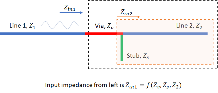
The via stub is basically a short transmission line with an open circuit load. As such, a signal propagating through the via will see an input impedance at the boundary of the via stub defined by an open-circuit load; this is one reason the via stub length is generally limited below a quarter-wavelength of the propagating signal (note the definition of bandwidth here!).
In terms of transmission line theory, this is a complex problem that has an iterative solution; read this article from Khongdeach et al. to see the actual solution method. The input impedance at the end of line 1 is a function of the input impedance seen at the stub/line 2 connection. The goal in this problem is to determine the critical length for the stub such that the input impedance of the vis stub is extremely large (infinity). For this reason, everyone just plays it safe and says to remove all via stubs on high speed lines. Unfortunately, every hole that needs to be drilled in a board adds cost, so you need to choose which stubs should be backdrilled and which to ignore.
Set a Via Stub Length Limit
The reality is that you don’t need to totally remove every via stub in your PCB, you just need to set the maximum stub length. This can be done in your design rules. As a rough approximation, the length of the via stub could be set to no more than 1/10th of the wavelength associated with the signal’s bandwidth (for digital signals) or the signal’s carrier frequency (for analog signals). Again, this is a rough approximation, but consider a 0.1 mm stub length as an example: this via stub length is appropriate for signals up to roughly 150 GHz (on a typical FR4 substrate). This is sufficient for most high speed protocols and commercial mmWave applications (e.g., radar or imaging).
If you need to design high speed/high frequency boards with short or removed via stubs, the routing and layout tools in Altium Designer® make it easy to set limits on via stub lengths. You can define limits as design rules, include backdrilling instructions in your drill table and fabrication documents, and prepare all other deliverables for manufacturing.
When you’ve finished your design, and you want to share your project, the Altium 365™ platform makes it easy to collaborate with other designers. We have only scratched the surface of what is possible to do with Altium Designer on Altium 365. You can check the product page for a more in-depth feature description or one of the On-Demand Webinars.
