What is a Schematic Netlist for Your PCB?
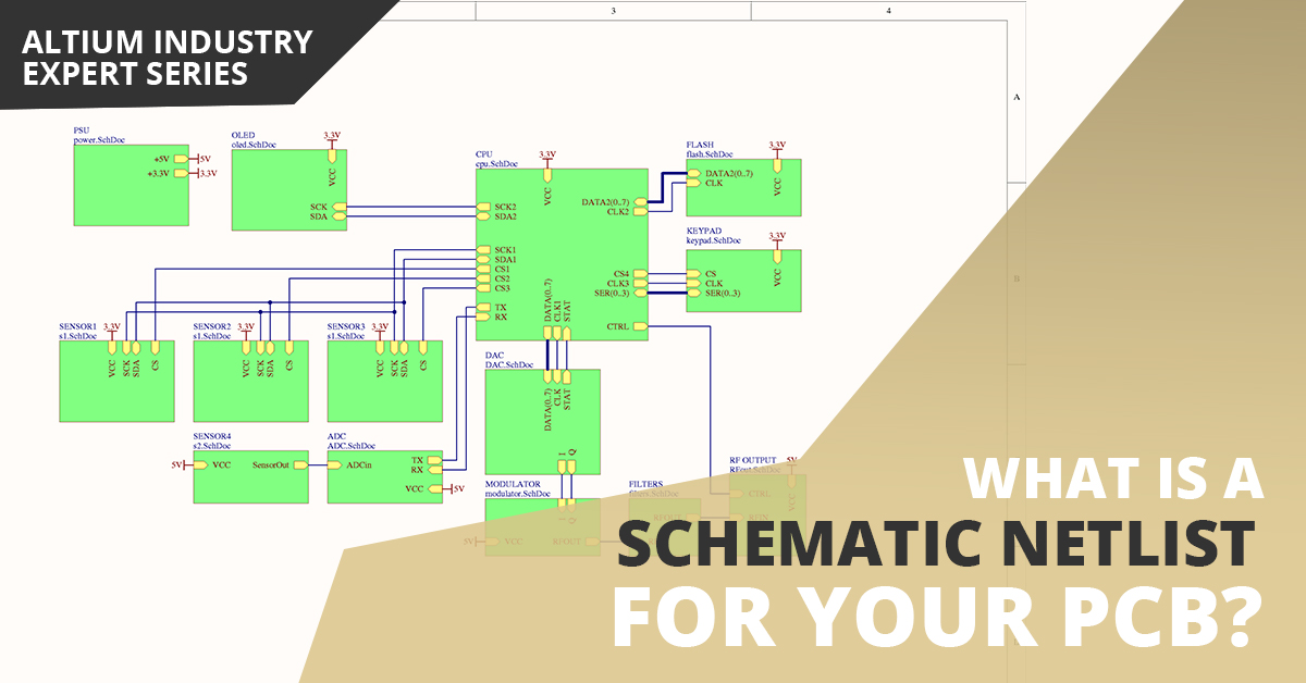
If you’ve created your next great schematic, there is a lot going on behind the scenes in your design software. The connectivity between components in your schematic can be reduced to a small number of logical and electrical identifiers. The schematic may provide a graphical picture showing connections between different components and pins, but to really understand everything about your design, you’ll need an important document.
A schematic netlist is one of the central pieces of information that will be used in multiple features in your design software to create a real PCB. Your schematic netlist provides both electrical connectivity information and reflects the functional structure of your design data in a single set of data. When you need to reuse your data or quickly define electrical connections in your simulation tools, your netlist will help you make the jump from schematic design to these other tools. You’ll also need to give your manufacturer a copy of your netlists as part of a design review. Let’s look a bit deeper at the exact structure of a netlist in your PCB design software.
What’s in a Schematic Netlist?
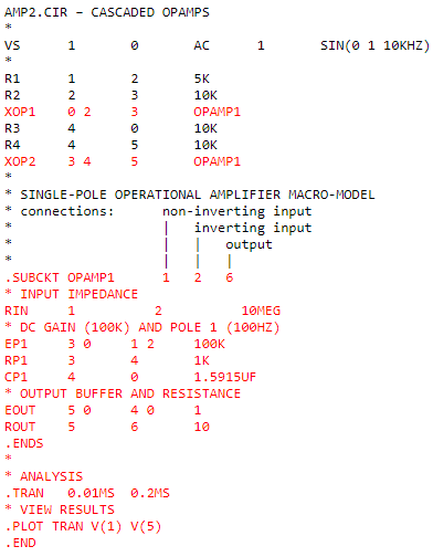
Before going further, there are different types of netlists used in EDA software for IC design or PCB design. These netlists can define logic, connections between components, and hierarchical relationships. They are a powerful tool for summarizing the structure and functionality of your design. A netlist does not contain graphical information—this is contained in the schematic document itself.
That being said, a schematic and its netlist go hand-in-hand; the netlist can be generated from a schematic, or schematics (flat or hierarchical) can be generated from netlists. With respect to the information in a PCB schematic, a netlist will contain multiple entries of data, in which each entry contains the following information:
- Net label: the name you give to a particular net in your schematic
- Reference designators: these designators are for the components connected on the net
- Pin numbers: each component on a net will have some pins, thus the pin number for each component on the net will appear in the netlist
If you know how to read a schematic netlist, you can see how a circuit is translated into a SPICE netlist when preparing a simulation. You can also troubleshoot any errors that might be found in netlists from third-party libraries.
Once you capture your schematic and import it into an initial layout, your schematic netlist data will be used to create the connecting lines seen in an unrouted layout. As long as you don’t need to make any further changes to your schematic, you can rest assured your design data will remain consistent as you route your board. However, you’ll still need to ensure your BOM and Gerbers match the information in your schematic and netlists before manufacturing.
How Fabricators Use Your Netlist
During a design review, data in your schematic netlist will be compared against your Gerbers, BOM, and schematic data. It is common to see discrepancies between a netlist and one or more of these documents. Most likely, this simply results from exporting a netlist and BOM before your design is completed; a last-minute design change before sending off your design requires rebuilding your BOM, netlist, and Gerbers to ensure all the data is consistent. While this might sound repetitive, it’s better than using a low-quality manufacturer and receiving a batch of defective boards in the mail.
Fabricators will also use your netlist to define requirements for bare board tests. The connectivity in the netlist is programmed into the test fixture used for the bare board testing process. Using the ODB++ data file format is a preferred format for manufacturing, as the netlist can be generated from the package. Otherwise, you’ll want to send an IPC-D-356 netlist along with your Gerber files, since this can be used for a thorough comparison before bare board fabrication.
Don’t Ditch Netlists From Your Old Projects
Design reuse is nothing new and spans everything from keeping frequently used libraries or circuit blocks. Importing design data from a different EDA application into your desired platform can be a difficult prospect. Your next design might be a variant of an old design, or it might require referring to certain functional blocks in the original schematic/layout. Keeping the netlists from your old projects can help you rebuild them in a new design platform, especially if the original layout and/or schematic data is corrupted or inaccessible.
Because the data placed in a schematic netlist is highly structured in a particular format, different design platforms can reuse each other’s netlists when building a new design. As long as you have models, schematic symbols, and PCB footprints for the components in the old design, you won’t need to manually rebuild the original design in your new software. While you could read off the net names, reference designators, and pin numbers from your netlist, you’re much better off working with design software that can help you quickly rebuild a design from an old netlist.
The schematic design and simulation features in Altium Designer® will now automatically compile your schematic as you engineer your new design. You won’t have to manually compile your project documents or worry about netlist discrepancies in your projects. With Altium Designer, you can easily import design data from other EDA platforms, which saves you time when reusing old designs. You’ll also have access to a broad range of tools for managing component data and preparing for production.
Now you can download a free trial of Altium Designer and work with the industry’s best layout, simulation, and production planning tools. Talk to someone at Altium today to learn more.
