Voltage and Current Waveforms on a Series-Terminated Transmission Line
In both of our books, Right the First Time, A Practical Handbook on High Speed PCB and System Design, Volumes 1 and 2, as well as in our on-site and public courses, we talk about the value of a series-terminated transmission line. With this type of transmission line, no power is being used unless the line is being charged up. This enables a lot of computing with a minimum of power. But having a clear understanding of how this type of line operates can be confusing and a bit daunting. In particular, visualizing how this operation works can be challenging. The purpose of this article is to clarify the operation of this transmission line and provide graphics that demonstrate it.
The Basics
Series-terminated transmission lines are the primary method for connecting CMOS devices with unmatched output impedance. In the following discussion, all the devices referred to are CMOS devices. CMOS devices actually led to ECL technology's demise because with ECL, no matter what was done, the line always drew power and caused severe cooling problems with large machines.
Figure 1 is a typical 5V CMOS driver with a 50 Ohm transmission line connected to a passive CMOS receiver.
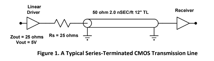
A passive receiver means that it simply responds to the voltage waveform presented at its input. For the purposes of this explanation, the CMOS receivers look like very small capacitors that are considered to be open circuits. Here, the line is about 12” (30 cm) long. The energy in a PCB travels approximately six inches per nanosecond. So, this line is about two nanoseconds long.
The schematic representation of the transmission line in Figure 1 is shown in Figure 2.
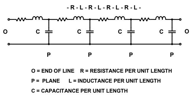
As can be seen, there is capacitance, resistance, and inductance distributed along the length of the transmission line. As noted in previous articles, these elements are referred to as parasitics, and they establish the behavior of a transmission line with the ratio of inductance per unit length to capacitor per unit length. Note that the substrate's parasitic conductance and loss tangent have been ignored for the moment as they are not so critical to understanding the basic shape of voltage and current waveforms. At sufficiently high frequency, but not so high that we care about skin effects or copper roughness, the inductance and capacitance determine the impedance of the line, as shown in Equation 1.

Note: When selecting drivers for series-terminated transmission lines, the driver's output impedance must be equal or less than the impedance of the transmission line.
In Equation 1, the inductance per unit length is expressed as Lo, and the capacitance per unit length is expressed as Co. (These two variables can be determined for a given transmission line type using a tool such as a 2D field solver). The equivalent circuit at T0 is the voltage source, and Figure 3 is the equivalent circuit when the transition from a logic 0 to a logic 1 begins.
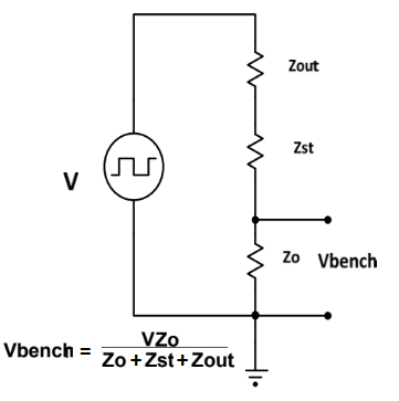
The voltage divider is formed by the combination of the driver output impedance and the series termination in the upper part and the impedance of the transmission line in the lower part. When the series termination has been properly chosen, the combination of Zout and Zst will be the same as Zo. In this example, both are 50 ohms.
Figure 4 shows the voltage and current waveforms for the series-terminated transmission line in Figure 1 as the driver switches from a logic 0 to a logic 1.
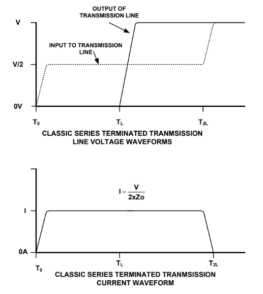
The voltage waveform starting down the series-terminated transmission line is V/2, which represents half the supply voltage. So, outbound, the capacitance is charged to V/2. This is represented by the current waveform shown in the lower portion of Figure 4 and can be shown by V's easy calculation over the two resistances in series.
Note: Ohm’s law describes the relationship between the current through a resistance and the voltage across it. Basically, the law states that the current in amperes is equal to the voltage in volts across a resistance divided by the resistance in ohms.
When the current gets to the far end of the transmission line, which is an open circuit with a shunt capacitor, the voltage doubles to the full scale value of V. The EM field is reflected back from the open end of the transmission line, and it is charging the capacitance up the rest of the way to V. When the EM field arrives back at the start of the line, the capacitance is fully charged, and the current goes to zero. This is seen in the lower part of Figure 4.
Important things to keep in mind about the operation depicted in Figure 4 include:
- The current waveform on the bottom of the graphic lasts two times the electrical length of the transmission line.
- The maximum current drawn from the power subsystem is set by the Zo of the transmission line and the supply voltage.
- The product of the current waveform and the voltage waveform at the input to the transmission line is the power that must be supplied by the power subsystem.
- The frequency content of the waveform is not set by the clock frequency.
Summary
The lowest power consumption method for high-speed logic signaling involves using a series-terminated transmission line. This is the lowest power consumption method because energy is only consumed in the circuit when a logic line is switched from a logic 0 to a logic 1.
Would you like to find out more about how Altium can help you with your next PCB design? Talk to an expert at Altium and learn more about making design decisions with ease and confidence.