Using Terminations To Control Reflections
In a previous two-part article, I discussed reflections, their origins and what they do to a signal using a typical unterminated 5V CMOS circuit as an example. As noted previously, this information applies to any logic family. This article will focus on how reflections can be controlled through the use of different terminations. Included in this discussion will be a description of the properties of those terminations and which work best in specific design implementations.
A Quick Overview
In the above-noted article, reflections and their behavior on a transmission line were discussed. In essence, it was demonstrated that the EM energy traveling down a transmission line will reflect along that line unless it is absorbed. The two types of reflections—overshoot or undershoot—were discussed, and data was given that showed undershoot is the primary issue of concern.
Just to review, in the upper portion of Figure 1, there is an unterminated 5V CMOS circuit driving a 50-ohm transmission line.
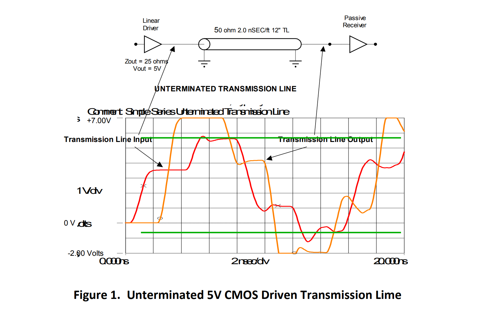
This circuit is fast enough that the reflected energy on this line causes the voltage that appears at the input to the load to be double the voltage level that started down the transmission line. During this process, the doubling exceeded the maximum allowable “1” voltage of +5.7 volts.
The bottom portion of Figure 1 shows both the rising and falling edges of the sample circuit. The falling edge also doubles and goes below the ground by more than 2 volts which exceeds the volt limit of -0.7V.
The two horizontal lines show the maximum allowable signal swing.
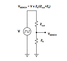
The reason for the excessive voltages is that the size of the signal that started down the transmission line was too large. When it doubled, the resulting voltage was too large. The value of the voltage that started down the transmission line is determined by the voltage divider formed by the output impedance of the driver and the impedance of the transmission line as shown in Figure 2.
Series and Parallel Terminations
There is something that can be done to make the two impedances in the above-noted equivalent circuit the same size. To accomplish this, the 5-volt starting signal will be divided in half and the signal that starts down the line will be 2.5-volts which is precisely just what is needed. Figure 3 shows how this is done.
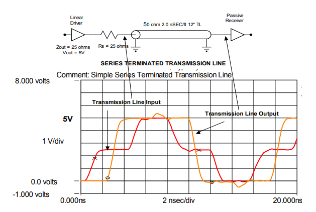
The divider ratio is adjusted by adding a 25-ohm resistor to the output of the driver. This is an example of a series termination.
As before, the 2.5V signal traveled down the transmission line arriving at an open circuit. This open circuit did not absorb the energy in the EM field. On the outbound trip, the parasitic capacitance of the transmission line was charged to V/2 or +2.5 volts. On the return trip, the parasitic capacitance was charged the rest of the way up to +5 volts. When the EM field arrived back at the source, it encountered the equivalent circuit shown in Figure 4.
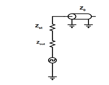
In Figure 4, the Zout is 25 and Zst (series terminator) is 25 ohms, totalling 50 ohms, and the voltage source is a short circuit. The transmission line impedance is 50 ohms. The effect is to provide a perfect transmission. The 50-ohm termination absorbs all the energy in the returning EM field so there is no reflection. This means that the circuit is stable at +5 volts. When the signal switches from a logic 1 to a logic 0, the same events take place. The load is provided with a square wave that was intended, and the input voltage rating of the part has not been violated.
Thus, the circuit in Figure 3 is said to have been “series terminated.” The resulting switching is often referred to as reflected wave switching because data becomes good all along the line only when the reflected wave passes by on its way back to the source. As can be seen, the voltage waveform at each end of the line is different. Only the load end of the line has valid logic levels at all times. Anywhere between the driver and the load, the voltage levels are halfway between a 1 and a 0 for some period of time. This is an invalid logic state. As such, edge-sensitive loads such as clock inputs cannot be located anywhere except at the end of the line farthest from the driver.
The reflected wave switching in Figure 3 is the basis for the PCI bus. It is the lowest power method for doing high-speed signaling. However, there are limitations when it is used for a bus such as PCI. The limitation is the duration of the two bench voltage levels while the signal makes a round trip on the bus.
Until this “dead time” elapses, no logic operations can be performed. This is why the original 33 MHz PCI bus had a bandwidth limitation. The amount of fast CPU performance that was available to the user was limited. The original 33 MHz PCI bus was allowed to be 30 inches long. The round trip delay on such a bus was 10 nanoseconds. The total time in a clock period is only 30 nanoseconds. On each switching edge, 10 nanoseconds is consumed as dead time. This leaves only 10 nanoseconds for the two logic levels. Increasing the clock frequency does not reduce the dead time. It only reduces the “data good” time.
We evolved from 33 MHz PCI buses to 66 MHz and 100 MHz bus systems. This is possible because of the following:
- The 66 MHz PCI bus specification states that the maximum bus length cannot exceed 9 inches. The round trip delay of this bus length is 3 nanoseconds. Out of this 15-nanosecond clock period, only 6 nanoseconds is used as dead time, 9 nanoseconds remain for logic operations. This is enough to accommodate the switching needs.
- The 100 MHz PCI bus has a clock period of only 10 nanoseconds. In order for this to work, the bus length is restricted to 5 inches or a round trip delay of 3 nanoseconds.
The foregoing discussion raises some interesting points. In order to use series-terminated logic in a bus organized system, it is necessary to reduce the system size as the clock frequency increases. This minimizes the dead time. At clock frequencies above 100 MHz, it becomes difficult to build meaningful systems of this kind. So, how is it possible supercomputers with clock frequencies over a GHz work?
If we assume that the EM energy is absorbed at the load end of the line by placing a termination there as shown in Figure 5, the events in the first part of the operations are the same as all of the previous examples.
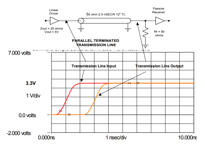
The +3.3 volts bench voltage is launched down the transmission line as the signal. 2 nanoseconds later, the EM field arrives at the load end of the line. Figure 6 depicts this for both the rising and the falling edges. There are the same waveforms at all points along the transmission line. It doesn’t appear that there are any illegal logic states or reflections.
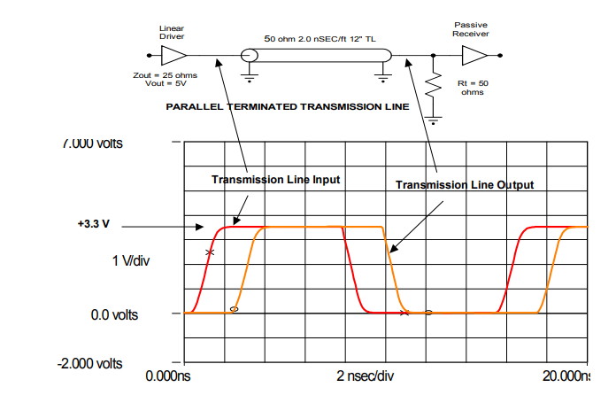
Unfortunately, because this is a 5-volt CMOS circuit, the minimum logic 1 for this family is +4.2 volts. The logic 1 in Figure 6 does not reach this level. Even though there are no reflections, the circuit will not work, so something must be done to raise the logic 1 level. The divider formed by the output impedance and the line impedance set the logic 1 level. One of these factors needs to change. It is difficult to change line impedances enough to remedy this problem so the driver output impedance needs to be reduced. Figure 7 depicts this.
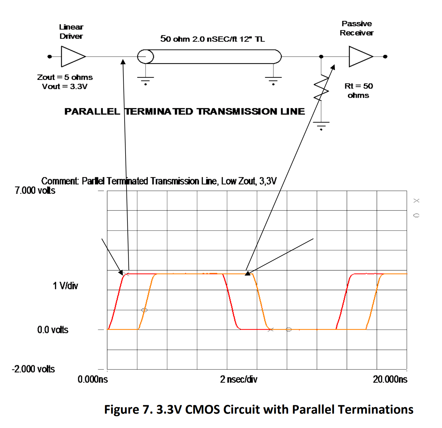
A new driver has been located with an output impedance of 5 ohms. This time the circuit has a 3.3-volt CMOS driver. As can be seen, the bench voltage which is the logic 1 is 10/11 of V or 3 volts. This is a proper logic level 1 for this circuit. All of the conditions have been met and there are no illegal logic states. In addition, a load can be placed anywhere along a transmission line with the assurance that it will always see a proper logic signal. This is called a parallel termination. It is the terminating method used for all very high speed logic paths. However, this signaling protocol also has its drawbacks in terms of power consumption. With the 3.3 volt signal swing, the power per signal line approaches 1/5 watt which is far too high to be used in practical systems. Because of this, the signal swings of all logic families intended to be implemented for parallel termination are small. For example, ECL signal swings are approximately 1 volt; GTL signal swings are 800 millivolts and LVDS signal swings are 400 millivolts.
The foregoing low level logic families work very well at high speeds. But, due to the small signal swings, they do not have a very big noise margin. As a result, noise management becomes a very important part of the design process. This is especially true when there is a mixed logic system that contains 3.3 volt or 5 volt CMOS circuits.
It’s important to remember that when a parallel termination is being used, the bench voltage is the logic 1 voltage. In order to create a logic 1 voltage that is large enough for proper operation, the output impedance of the driver must be much less than the line impedance.
Other Types of Terminations
In addition to series terminations and parallel terminations, sometimes other terminations are offered up as solutions to reflections. Those terminations include:
- AC Terminations.
- Diode Terminations.
- Thevenin Terminations.
- Thevenin networks as pull ups or pull downs.
- Series and Parallel Terminations used on the same net.
These terminations and their technological validity, or lack thereof, are examined below.
AC terminations are sometimes suggested as a way to control the voltage doubling at the open end of a transmission line. An AC termination attaches the parallel terminating resistor to the end of a net with a small capacitor. The objective with this approach is to provide the termination during the times that edges are switching and disconnecting it when the logic levels are “steady state.” This method was originally devised when TTL edges got fast enough that they exceeded ¼ TEL (transistional electrical length) and caused excessive voltages at the inputs of gates. When an AC termination is attached to the end of a net, the result is a rising or a falling edge that has an RC time constant that effectively slows down the edge while it limits overshoot. If the edge degradation is acceptable, an AC termination might be the way to cope with fast edges.
In Figure 8, the upper portion of the figure shows the same circuit contained in Figure 1 but with an AC termination.
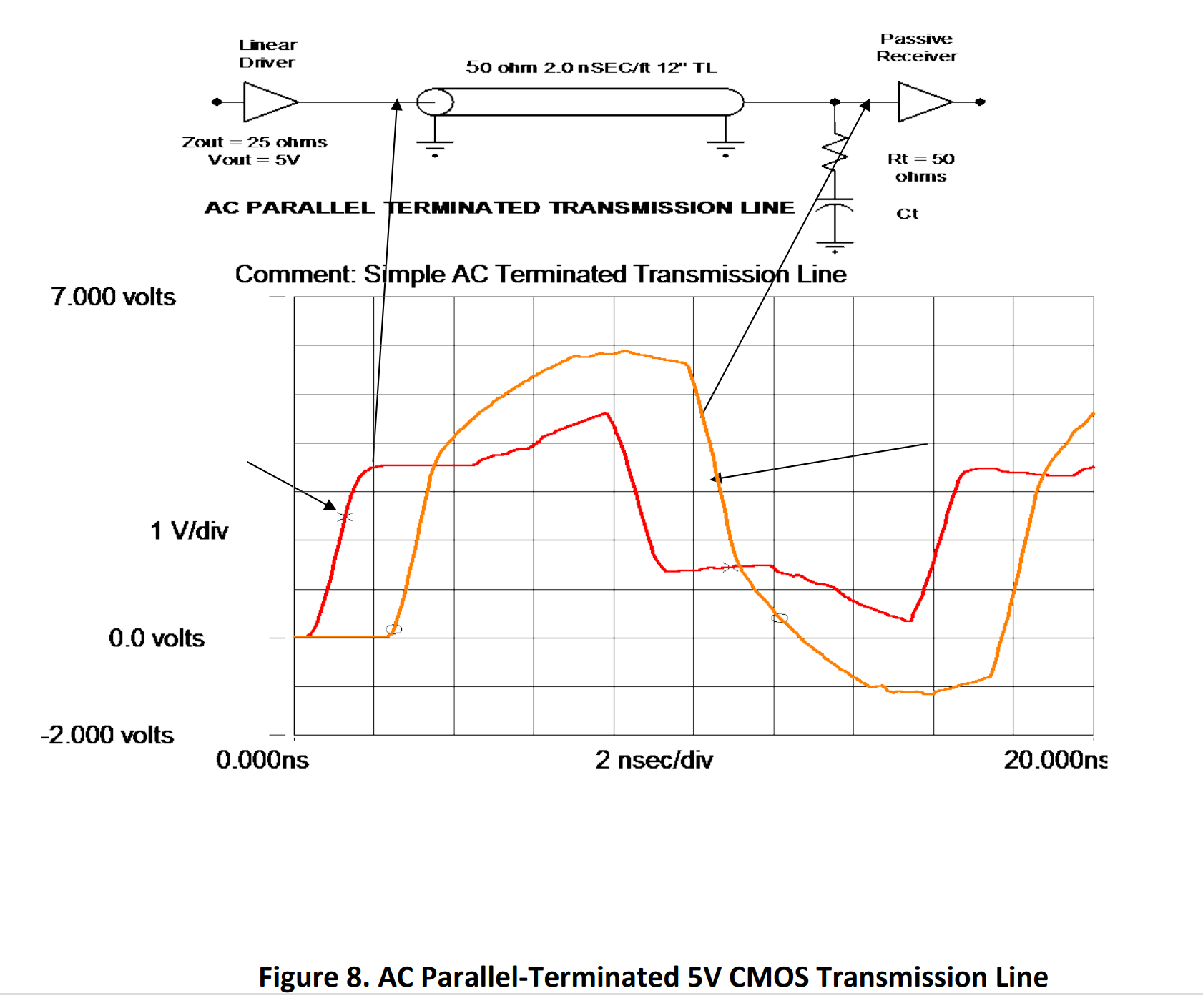
As can be seen, when the value of the resistor and capacitor is chosen such that the overshoot does not exceed Vdd +0.7 volts, the signal is beginning to look like a sine wave and the edges are no longer sharp.
If the clock frequency is increased much beyond the 66 MHz in this example, not only does the waveform become more like a sine wave rather than a square wave, it is no longer capable of maintaining the required signal swing. This problem occurs when trying to use an AC termination with DRAM arrays. It is not a well-behaved methodology at high clock rates and should instead be considered only as a “band-aid” solution for a circuit that should have been designed at the onset with a true series or parallel termination.
Diode terminations at the receiver end of a transmission line in lieu of a resistor termination are
another instance of a band-aid approach. Instead of designing transmission lines with proper
terminations that prevent overshoot from becoming excessive, a pair of diodes is attached between the signal line and the two power rails and is oriented such that when overshoot exceeds Vdd, one diode turns on as a clamp. This is shown in Figure 9.
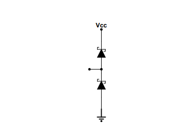
When the overshoot attempts to go below Vss (Voltage source supply), the other diode turns on as a clamp. This does work however the diodes must be Shottky diodes in order to turn on quickly enough. In addition, the cost per line of this particular approach is quite high.
Parallel terminations described thus far have been connected to ground. This is a symbolic ground as the actual parallel terminations always connect to a special terminator voltage not ground, Vdd (Voltage drain) or Vee (Voltage emitter). In the case of ECL, which operates between ground and -5.2 volts, the terminating resistors are actually connected to a special Vtt (Voltage termination) supply that is -2.0 volts. GTL terminations connect to +1.2 volts while parallel terminations for 2.2 volt CMOS connect to +1.1 volts.
When using the above-mentioned logic families, it is necessary to add a power supply and a power plane to supply the needed terminator voltages. If there are only a few circuits that need parallel terminations, as is the case when PECL is used for an interface to a transceiver, this equates to a large expense for just a few lines.
Another approach to this problem is to use a two-resistor network to emulate the terminator impedance and the terminator voltage. This is referred to as a Thevenin equivalent and it is depicted in Figure 10.
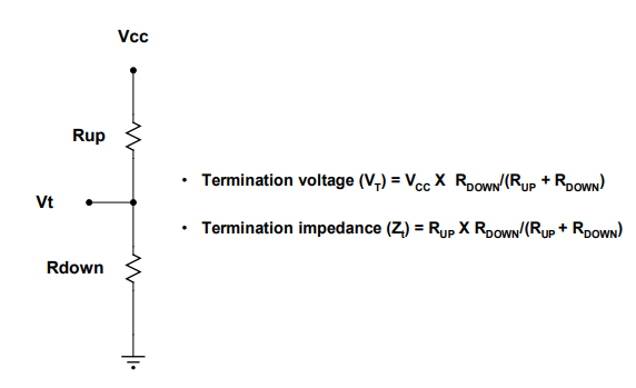
To determine the values of the resistors required to create the equivalent voltage and impedance, it is necessary to solve the two equations featured in this figure. Here, Vcc is the voltage from a power supply connected to the collector terminal of a bipolar transistor. Vt is the voltage transformer.
A Thevenin network can be used to create a pull up to some voltage other than Vdd or a pull down to some voltage other than ground. An example of this is the resistor network on a VME bus backplane.
Figure 11 is an example of a pull up network.
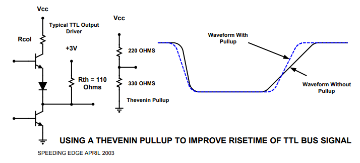
A TTL output has an unsymmetrical output. The impedance of the output as it switches from a 1 to a 0 is much lower than when it switches from a 0 to a 1. Because of this lack of symmetry, the rise time can be too slow to satisfy timing margins. Adding a pull up to +3V, which is the maximum 1 for TTL, provides more power to the charge up line. This yields an improved rising edge while the falling edge is only moderately degraded.
Table 1 depicts all the ways to terminate a transmission line and their specific operating characteristics.
Figure 12 shows the location of each termination on a network.
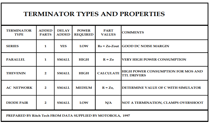
While five types of terminations are listed in Table 1, only three of them are really useful. These include: series termination, parallel termination, and Thevenin equivalent parallel termination.
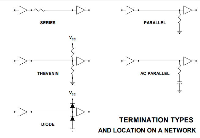
All of the logic that is intended for use in high speed signaling is capable of being handled with one of these foregoing terminations. If a design rule set seems to call for AC terminations or diode terminators, it’s a good idea to go back through the decision making process to determine why their use has been specified. It’s more than likely that an error was made when the design rules were devised.
In almost every one of our classes, there has been the perception that both a series and a parallel termination are needed on a network. Figure 13 is an ECL net that has a series termination at the output of the driver and a parallel termination at the load end.
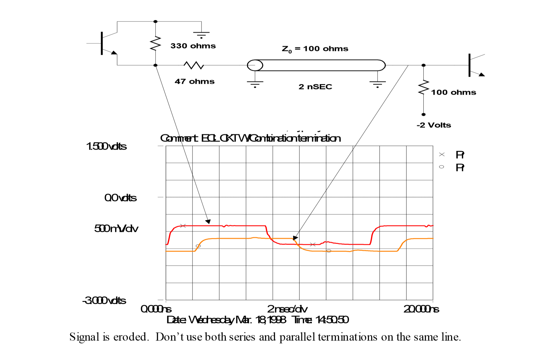
As can be noted, the signal that arrives at the load never gets up to the -0.8 volts required for an ECL logic 1. This occurs because the series termination and the transmission line have divided down the output signal before it starts down the transmission line. Because there is a parallel termination at the load end, there isn’t any way for this signal to double as a way to reach a proper logic 1. In this instance, the “series termination” is serving as a current limiting resistor which is what was wanted.
Unfortunately, the transmission line also sees it as a series termination.
Exceptions to the Rules
As often happens in designing high speed electronics systems, there are exceptions to the foregoing rules. There are instances when a termination is needed at both ends of a transmission line. Two examples of this are a video driver that has an emitter follower for an output as well as OC-48 drivers.
The design specifics for both of these are described below.
In the case of a video driver, emitter followers have a tendency to oscillate. A common method for preventing this is to place a small resistor in series with the emitter as it drives the transmission line.
When this is done, the signal problem is overcome by designing the video amplifier such that it creates a larger starting voltage.
With OC-48 drivers, there are small reflections, created by imperfections such as connectors in the transmission line path. These small reflections arrive back at the driver which is usually a pseudo current source. This means that the driver has a high output impedance. The energy in the afore-mentioned small reflections is reflected by the driver’s high impedance and travels back toward the load. Upon arrival at the load, the reflections add to the jitter. By adjusting the output impedance of the driver such that it exactly matches the line impedance, the small reflections are absorbed and jitter is improved. The two ends of the transmission line are terminated such that the driver end has a series termination and the load end has a parallel termination. Here, the driver design must account for these factors. However, it should be noted that with commercially-available components, there is no way to adjust the driver characteristics such that both a series termination and a parallel termination can be used.
Summary
For controlling reflections, the two viable options are parallel terminations, serial terminations or, with certain logic families, Thevenin-equivalent parallel terminations. While other types of terminations are in existence, they are often band-aid implementations that are far less preferable then initially designing circuits with properly placed parallel or serial terminations.
Have more questions? Call an expert at Altium or discover more about transmission lines and terminations in high-speed design with Altium Designer®.
References:
Ritchey, Lee W. and Zasio, John J., “Right The First Time, A Practical Handbook on High-Speed PCB and System Design, Volume 1.”