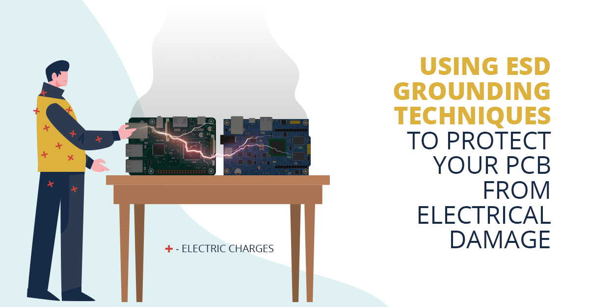
Using ESD Grounding Techniques to Protect Your PCB from Electrical Damage
I was in high school before I considered engineering as a career outside of the engine room on any Star Trek show. Although, subconsciously I was definitely interested in it. The signs were there early considering I could name all the chief engineers from Star Trek. The deal was sealed though when I was ridiculously excited to receive an ESD grounding wrist strap bracelet as a gift. Don’t have one in your jewelry box? Well, it’s composed of elastic webbing with a wide metal strip that goes against your skin and a cable with an alligator clip that you attached to ground. We only had dial-up internet at the time, but that didn’t stop me from spending hours waiting for pages to load so I could figure out how to ground myself. Armed with my wrist strap bracelet, I convinced my friends to hire me to upgrade their computers’ RAM, or just let me open up their computer.
Although ESD grounding can be as simple as touching something metal and not scuffing your feet, it’s best to be grounded before handling anything ESD sensitive.
Using grounding to protect from electrostatic discharge is necessary at many stages in your product development. When you’re handling sensitive products, like RAM cards, good practice includes using an ESD workstation mat and grounding yourself. You can also provide grounding protection for your products by designing them properly. It’s better to apply good grounding practices to your PCB design and reduce the dependence on the safe handling practices. As Spock would say, it’s illogical to assume that all future customers or installers will obsessively ground themselves when handling sensitive products.
Use ground planes
There are a number of ways to utilize a grounding strap to your wrist for electrostatic discharge protection, but first and foremost is using a point ground plane. Although it’s not always feasible to use a multilayer design, the ground plane can really help you out if you’re concerned about ESD protection. As you know, a sudden surface voltage discharge will induce electromagnetic fields. A properly connected ground plane can reduce the electrical damage from this by routing the current away from sensitive components.
Using a ground plane gives you another way to reduce the area of loops in power to ground traces. When you reduce the area of loops, you’ll decrease the total EMI induced within the loop area. That, in turn, decreases the corresponding current that can flow into components where it shouldn’t.
Protect your ground planes
For all the good a ground plane can do, it can also act as a direct path to your sensitive components if an ESD sensitive pulse discharges directly into it. To prevent this sort of static dissipative damage, remember to use TVS circuits between the power and ground on sensitive components to divert the induced currents. When implemented correctly, the voltage differential experienced by components will be held to the clamping voltage of the TVS.
You can also use high-frequency bypass capacitors between power and ground on sensitive components. The capacitors will reduce the charge injection and voltage differences between power and ground. Keep those capacitors and your TVS close to the components you are worried about protecting against static charges.
Additionally, you should use a copper land when you are attaching connectors to your PCB. Make sure the land is separate from the PCB ground, or you just introduced a nice, low resistance path for ESD to reach all your components, even though you put all that other electrical ground protection in place. And, in general, you should minimize path lengths whenever you can.
Use a chassis ground
Similar to grounding yourself and a computer tower case before you start pulling things out, you can ground the external casing of your product. By allowing your board and chassis to share a ground, you can improve the grounding of the entire system. One of the easiest ways to implement a chassis grounding is to include a “chassis screw” that connects the ground plane to the chassis. However, you need to make sure you’re using adequate standoffs so other components aren’t crushed or shorted to the casing when the PCB is screwed in.
Using a chassis screw can help you ground your PCB to your external casing, and then to earth ground.
Additionally, grounding with a chassis screw makes ESD protection circuits more effective when you’re using transient voltage suppression at inputs. Remember, you’ll want to separate the chassis ground from the digital and analog ground by using inductive components. That way, a discharge into ground won’t accidentally be shared with all your other components.
If you are designing high-speed circuits, you know that they are always more difficult to optimize for performance. This is especially true if you’re routing across multiple ground planes, like a chassis and a PCB layer. The best case scenario is that you can connect the chassis ground directly to an earth ground. If that’s not an option, you should keep all of the ground planes tightly coupled to each other. That will help to minimize any “ground shifts” around key components.
When you do use an earth ground to your chassis, Texas Instruments recommends that you should keep it “immediately adjacent” to both the ground on your TVS and to the ground of the expected ESD source, usually a connector shield on the input
Well meaning fingers can do a lot of unintentional damage when installing, cleaning, or inspecting a PCB.
Incorporating good grounding into your design can save you from a lot of damage caused by awkward or inquisitive fingers; however well-intentioned. And while it adds an additional layer of complexity to plan for your casing and stand-offs, it can save you a lot of time respinning your design. One PCB tool that can help manage the added complexity is Altium’s 3D clearance checking. By letting Altium manage the physical spacing of your board and case, you can focus on the rest of your design. You can get started with Altium now, and get it right the first time!