Understanding Your PCB Netlist

Understanding Your PCB Netlist
There are several different ways that netlists are used at various stages of the electronics development process. Netlists may have different purposes and may have unique data formats, but they all provide a similar function; they list the connections of an electronic circuit. This is important for a variety of fundamental tasks in electronics and PCB layout design. Your netlist is used graphically in your schematic editor as well as your PCB layout editor. It’s also used in SPICE simulations to define loops and nodes for use in iterative solution algorithms.
The data in a PCB netlist may look simple and unintuitive, but it can be a big help when reusing an outdated design or importing design data from another program. Most designers are probably familiar with a schematic netlist, but there are multiple netlists for any PCB design. Let’s take a look at the power of netlists and how you can bring them into your design process.
The Schematic Netlist
Since Altium Designer® is an integrated system, much of the data being synchronized between the schematic and the PCB layout happens behind the scenes. The “Update PCB Document” on the schematic side, and commands like “Validate PCB Project”, “Update Schematics”, or “Import Changes” from the PCB side keep the netlist updated and the connectivity synchronized.
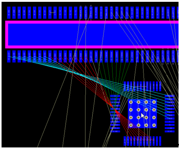
The result of this project synchronization is displayed to the designer as “Connection Lines”, which is how the netlist is graphically displayed in the layout (see the image below). If you’ve paid attention to the automatically-assigned net names in Altium Designer, you’ll notice that these names refer to some connection in the schematic. These nets are then mirrored in the PCB layout.

Just so you know what a netlist looks like, the image below shows a small portion for a design. This is just a simple text file (ASCII file) that can be opened by any text editor.
_1.png)
Without getting too much into the gory details, a netlist specifies different ports on components and the net to which they are connected. This is all specified in a standard format, making it very easy for different programs to read each other’s netlists. This leads us to one great benefit of keeping an up-to-date netlist; you can import a netlist from another design into a new project.
Importing a Netlist
Imagine you are being asked to design a board, but the schematic has been created using a different software package. Knowing that a PCB layout is driven by a netlist—and maybe a Part List, as well—couldn’t we use these inputs from the other system? Can we start a layout with no schematic? Theoretically, the answer is YES!
Altium can import a simple ASCII netlist and the layout can be done with no synchronization between the two systems. One of the threads in the Altium User Forum describes this process. Before you try something like that, be warned that it can be tedious and error-prone to keep up with circuit changes along the way, and Altium provides better solutions for this situation.
Instead of importing a netlist, Altium has developed a sophisticated “Import Wizard” that can work with various types of design files instead of simple netlists. Here is a current list of design file types which Altium can take advantage of:
.png)
Very impressive, but we have veered away from the subject of netlists.
Let’s get back on track…
Exporting a Netlist
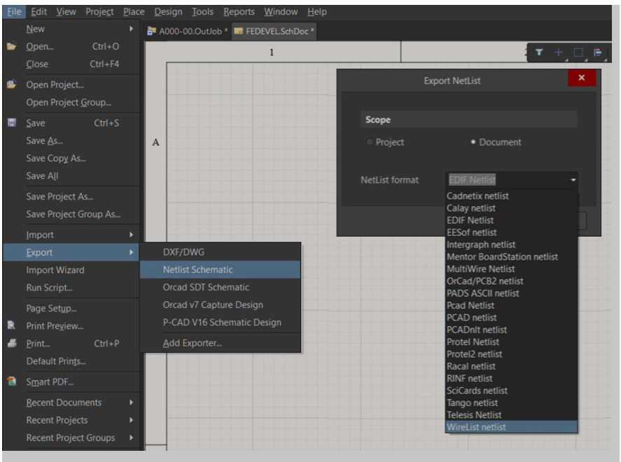
As we saw in the last section, Altium can take advantage of netlists and design files from other systems to make our jobs easier and reduce the risk of error. You might be wondering, “Can we go the other direction and EXPORT a netlist?” Of course we can!

Netlist Checking by Manufacturers
We have been looking at the netlist as a form of data that describes the connectivity of an electronic circuit. It keeps the schematic and PCB layout synchronized with each other in the integrated Altium Designer system. Now we will look at two other types of netlists that are used in the manufacturing process.
The Gerber Netlist
If you send your design to a bare board fabricator using the ODB++ data format, it will have a netlist included as part of the package (or a netlist can be generated from the package, if that is a more accurate way to describe it). If you are still using Gerber Data, however, the CAM department will GENERATE a netlist directly from the Gerber Data to be used for the bare board test at the end of the line.
When you order bare boards from a supplier and receive a quotation, you might notice a cost for NRE, which means “Non-Recurring Engineering”. These are one-time costs, no matter how many times you order that revision of the board. One of these costs is the “bare board test”, and the test fixture used for this part of the process needs a netlist to know what the connectivity should be. The manufacturer will generate a netlist from your Gerber Data to compare with the finished bare board. This will ensure that the final board connectivity matches the input data you sent to them.
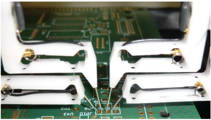
Here is an example of a “flying probe” bare board tester:

The IPC-D-356 Netlist
The “Bare Board Test” compares the manufactured board to the original Gerber Data, but what if the Gerber Data is wrong? That’s where our final netlist type can save the day!
The IPC (Association Connecting Electronics Industries) has developed another netlist data format called IPC-D-356, that can be used to compare the schematic netlist to the Gerber data. This comparison is performed BEFORE the bare board manufacturing job is started to make sure there is no discrepancy. Requesting this test will likely add to the NRE charge for the bare board quotation, but it will be far cheaper than manufacturing a bad batch of boards, especially if the error is not noticed until after final assembly, at in-circuit test (ICT).
The way it works is, you add “netlist testing” to the quote, with the understanding that this test will be performed BEFORE the bare board manufacturing is started. If any discrepancy is identified, the job will be placed ON HOLD until the discrepancy is resolved.
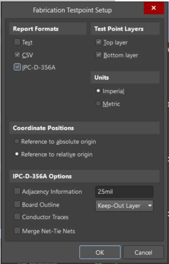
Altium OutJobs can generate this file automatically, and your setup can call it from either the OutJob “Fabrication Outputs” or “Assembly Outputs”, although currently it is confusing that Altium names this capability as a “Test Point Report”.

Remember that the netlists we have been exploring are similar; they describe or record the connectivity of circuits. There is another type of file that is often confused with netlists, which is the “Test Point” data file. This file is exported for an ICT fixture. A test point file lists at least ONE accessible node location for every unique net name that will be probed.
Summary
Although the schematic is a graphical way to describe a circuit, the schematic netlist records the connectivity in a data format that can be used by software and machines. Altium Designer can export netlists in formats that are used in the manufacturing and testing of the final product. Alternatively, you could import netlists and design files from other programs and begin using your old designs in Altium Designer.
For more information, take a look at the following links:
- Documentation for Altium’s Netlist Manager
- Documentation for Altium’s IPC-D-356 Netlist Support
- IPC-D-356 Standard – Bare Substrate Electrical Test Data Format
Would you like to find out more about how Altium can help you with your next PCB design? Talk to an expert at Altium.