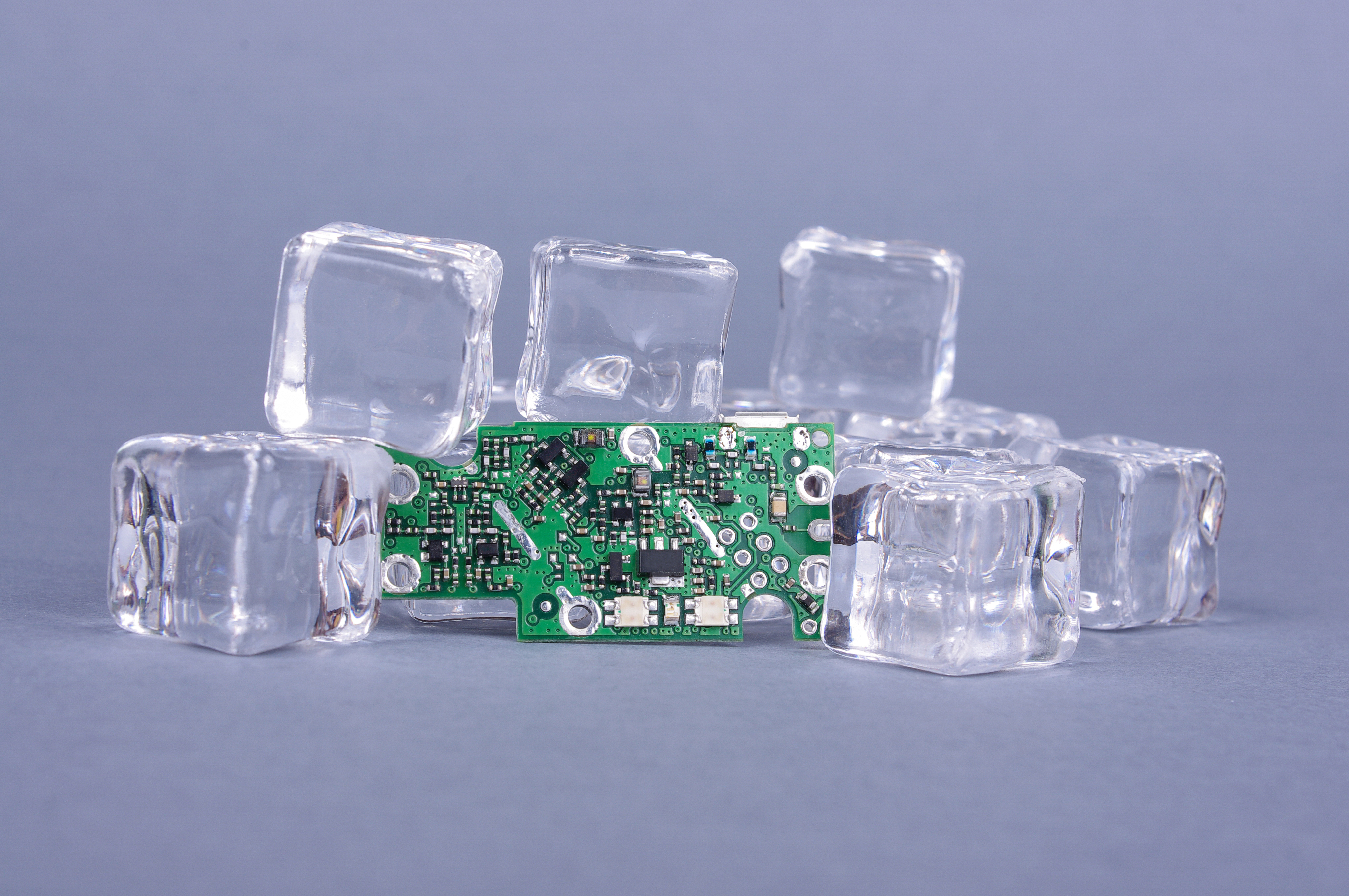
Thermal Management for Integrated Circuits
As anyone who designs and builds electronic devices knows, the device will generate heat when it’s switched on. Wherever current flows through an impedance, energy losses will manifest themselves as heat, thanks to thermodynamics laws, whether in components, connections, wiring, or the PCB. The greater the loss, the greater the excess heat generated.
While components with thermally enhanced packages are available to help manage any heat generated, the trend in electronic designs is for more compact devices with a greater concentration of components. Integrated circuit packaging is getting smaller to meet this trend but at the cost of poorer thermal properties.
In semiconductor devices, the component gates have been shrunk down to nanometer sizes, and a single die can now contain millions of gates formed from billions of transistors. Moore’s Law has marked this progressive miniaturization and predicts it will continue into the near future until a shift change in the underlying technology. While each new generation of smaller, faster devices offers the designer more features to play with, they generate more heat in the same component footprint.
Effect on semiconductors
Excessive heating of semiconductor devices can have several impacts on the operation of the device. The properties of the semiconducting material itself change with temperature due to electromigration effects. Outside of the device’s temperature limits, the device’s performance may not adhere to its specification and produce unexpected behaviors. Semiconductors rely on bonding for the connections from the PCB pads through to the die substrate, the integrity of these bonds can be compromised if exposed to high temperatures.
Another factor to consider is heat stress effects when the device is switched on, off, or subjected to pulsed loading effects. The devipower line’s rapid cycling as temperatures is reasonably slow-cycling due to the nature of the materials used and its thermal connection with the ambient environment. On the other hand, the die will be subjected to rapid temperature changes when it changes state, such as the power line’s rapid cycling.
Semiconductor devices are typically composed of the die bonded to an insulating substrate connected to a copper base plate. This heat stress can induce power-cycle life faults due to the thermal stresses distorting the different layers within the semiconductor device. The various materials used in the manufacture of the device may expand at different rates. This can lead to fractures or delamination in materials or the application of stress forces on the die caused by the expansion of encapsulation materials. Such effects can lead to the premature failure of the device, adversely affecting the reliability.
This can be summed up with the assertion that the higher the operating temperature, the lower the reliability. The datasheet for a device will provide a predicted Mean Time Before Failure (MTBF) at a specific temperature, typically standard room temperature. There’s a general (and very rough) rule of thumb that this MTBF halves for every increase of 10 oC in the operating temperature. This is based on historical evidence from chemistry, where the rate of chemical reactions tended to double with every 10 oC change causing an exponential increase.
The challenge is to extract the heat energy from the semiconducting material and dump it into the ambient environment as quickly and efficiently as possible to maintain the device’s reliability.
Device ratings
The datasheet for your semiconductor device will specify its operating temperature range. Usually, this will be 0 oC to 70 oC for a standard commercial product or potentially -40 oC to 85 oC for an industrial-rated part. Military spec parts with even more ranges are available if necessary but at a much greater cost per unit. In reality, there’s little difference between the various products; they are manufactured with a margin that means a commercial part can operate over the mil-spec range. It’s often down to more rigorous testing of the higher-spec components to certify they meet the required operating field.
The Absolute Maximum Rating (AMR) will define the operating limits, including the operating temperature and junction temperature. The device manufacturer selects these values based on providing the device’s acceptable serviceability under the worst possible operating conditions, including variations in supply voltages, variations in loading, signal variation, and the allowable environmental conditions. The AMR will be dependent on the user following any recommended operating conditions specified by the manufacturer.
Thermal resistance
For a semiconductor device, thermal resistance measures how the device resists the flow of heat from the junction to its outer surface. Designated with the symbol θ and measured in oC/W, the lower the resistance, the more efficient the device is at pulling heat away from the junction and out of the device where external cooling mechanisms can be applied. The units may seem a little odd. However, it’s pretty practical - the units are the temperature difference, in degrees Celsius, between the two stated points if you have 1 watt of heat. So 140oC/W θJA means between the semiconductor junction and ambient, you will have a 140oC temperature difference with 1 watt of heat applied at the junction.
Usually, the datasheet for a component will specify the junction’s thermal resistance to the ambient environment, designated θJA. Alternatively, it may be broken down into the thermal resistance from the junction to the case, designated θJC, and from the case to the ambient environment, θCA.
Therefore, the maximum junction temperature can be calculated using the device’s thermal resistance, the full power dissipated within the device, and the maximum ambient temperature.
The thermal resistance will depend on the amount of copper around the die, the materials used for encapsulation, the thickness of materials, and even the die’s orientation within the device.
One additional factor worth considering as an aside is the die material itself. The introduction of techniques that allow defect-free boron arsenide substrates produces a significant decrease in thermal resistance compared with traditional silicon-carbide-based materials and lower than copper. However, such devices are outside the reach, and budget, of the average electronics engineer.
Steady-State and Transient Considerations
An important point to bear in mind is that failure mechanisms due to excess temperatures are less likely to result from high steady-state temperatures. They are more likely to be caused by changes in temperature gradients, temperature cycle magnitudes, and the rate of change of temperature having a more significant impact. Semiconductor devices that handle pulses of power rather than steady-state power are more prone to heat-related failures. The message here is that how the device is operated is just as crucial as its operating environment. If the device is handling pulsed signals at a high frequency, it will require a more robust thermal management solution than handling a relatively slow-changing signal.
Thermal design has grown in importance with the increasing use of semiconductor devices in discrete components and the desire to pack these into smaller and smaller devices. Standard practice is to perform a steady-state thermal analysis on the device and provide the calculated cooling level based on the results’ results to achieve the required reliability. However, transient thermal analysis may well identify that this cooling level is insufficient based on the device’s real-world operating modes. The problem is that steady-state thermal analysis is far simpler and quicker to undertake. The temptation is to perform the steady-state analysis, add safety factors based on engineering judgment, or take a device and monitor temperatures out in the field to see if there will potentially be a reliability issue in the long run.
Heat dissipation solutions
The typical starting point for heat dissipation is to utilize the PCB itself as a passive cooling method. If space and component placement allows, then the use of copper PCB traces with their low thermal resistance is ideal as a low-cost heat management solution. The careful placement of copper polygons under and around the semiconductor can take away heat from the device and spread it across the rest of the PCB. This is particularly effective if the semiconductor device has been manufactured with a large area copper slug positioned under the die. The die rests directly on this slug and is exposed on the packaging’s underside to be located directly against the PCB’s surface to maximize heat flow. However, more complex semiconductor devices are manufactured with stacked die where heat extraction can be far more complicated.
An obvious downside is that the dissipated heat will affect the other components on the board. Conversely, any other hot devices such as power FETS can themselves dissipate heat into the semiconductor. Thermal analysis of the entire board will be essential to ensure that the overall thermal management solution will be effective. There will be no hot spots in any critical areas of the board that could affect temperature-sensitive components.
Heat sinks are another common technique for providing localized heat dissipation for semiconductor devices. The basic principle is to have a metal structure with as large a surface area as possible physically attached to the semiconductor device. Heat can then be radiated away from the device much more efficiently than relying on its small surface area radiating the heat. Typically, a thermal interface material is used to bond the heat sink to the semiconductor, which, in essence, is a bonding agent with a very low thermal resistance. A standard heat sink uses an Aluminum structure covered in fins to maximize surface area and provide a path for the warmed air in proximity to the heat sink to move due to induced convection currents. This occurs when the air temperature becomes sufficiently greater than the ambient air temperature.
If a heat sink alone will not provide the required heat dissipation level, adding forced airflow over the fins of the heat sink using a fan will replace the warmed air with ambient air quicker than relying on convection alone. It’s important to note that the device must be designed to allow an unimpeded airflow from outside, across the heat sink, and then back out of the cooling device to be effective. One drawback is that such an arrangement can draw in dust and contaminants into the device that may affect overall reliability or potentially reduce the heat sink’s thermal efficiency.
An alternative solution if space is limited is a heat pipe. Available as an off-the-shelf device, heat pipes provide a reliable and cost-effective method for the passive transfer of heat from a hot spot on the board to a colder location. Typically, a heat pipe contains a small quantity of heat-absorbing liquid, such as pressurized nitrogen, ammonia, or acetone. The fluid absorbs the heat and turns to vapor, which travels along the pipe to a condenser. Here it condenses back to its liquid form and returns to the cycle’s heat source to start again. The main advantage is it’s a passive component with no moving parts and no maintenance requirements. However, the costs can be high, and installing on the PCB can be challenging.
Other solutions, including liquid-cooled cold plates or Peltier effect cooling plates, are all possible options. Still, significantly greater cost and complexity, making them impractical for many consumers targeted device budgets.
PCB Heat dissipation recommendations
If you can utilize your PCB as a passive heat dissipation solution, here are a few recommendations to help make this as efficient as possible.
As the first step, review your design and see if there is an option to reduce the heat components. Changing components, redesigning circuits, or rethinking power supplies can often be successful strategies. Prevention is always better than cure.
Use as large an area of copper as your design will allow. If you are not constrained by board size, consider increasing the board area to get the extra surface area for heat dissipation purposes. Do not cover any copper that will be used for heat dissipation with a solder mask as this increases the overall thermal resistance, defeating the point of using exposed copper. Utilizing a multi-layer board, use areas across the multiple layers, and link them with numerous vias to maximize the thermal coupling between them. Thermal vias have the advantage that they increase the mass and area of the copper on the board, which reduces the thermal resistance and provides an improved heat dissipation with little effort, as long as you have the space to accommodate them in your PCB layout. These thermal vias need to be placed as close as possible to any heat source to be effective. Also, use a PCB with the thickest copper you can; this directly affects how quickly heat can conduct across the board.
Provide natural ventilation to the board so air can freely flow across the board’s surface, ideally in a manner that allows equal heating across the surface area. Hence, this minimizes the risk of any hot and cold pockets of stagnant air forming that could lead to uneven cooling.
If your PCB is installed in a casing, select a case made from a material with low thermal resistance and thermally couple the PCB to the case. Consider maximizing the case’s surface area with fins, ridges, or maybe a simply raised design motif. If your device’s casing allows, orientate the PCB vertically to take advantage of the natural tendency for hot air to rise and cold air sink, increasing the natural convection currents’ airflow rate.
If passive airflow cooling is insufficient, consider adding a fan that pushes ambient air onto the board or pulls heated air away. Ideally, the fan should be placed at one end of any natural convection currents path to reinforce this natural airflow rather than driving against it. Ensure that the air will be free to flow; it’s no use having the air inlet path on the device’s underside if it will be blocked when the device is placed on a soft surface. Also, consider using some type of filter if the forced air may contain dust or if the device will be operated in a location where airborne particulates or contaminants may be present.
Conclusions
Thermal management is an essential consideration in the design of electronic devices that include semiconductor components. The susceptibility of these parts to heat and the heat they generate themselves makes it a challenge to maintain the temperature at the core of the device with acceptable levels using techniques to manage the device’s outer surface temperature. The trend towards smaller packaged devices performing more functions exacerbates this problem. The solution is to include careful thermal analysis as part of the design process and adopt thermal management solutions as an integrated part of the design.
Would you like to find out more about how Altium Designer® can help you with your next PCB design? Talk to an expert at Altium.