Signal Integrity Simulations for Backplane Bus and Connectors
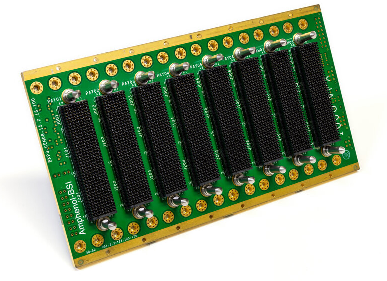
You’ll need a backplane to stack multiple cards in a rack-mount unit
The days of sub-Gbps data rates are long gone in most systems. Modern systems that interface with a large number of devices in a single enclosure will probably need a backplane, and those that do will likely run above Gbps data rates. Of particular importance is your choice of connectors, and it's important to verify your backplane bus/connector design choices with simulations.
Backplanes can be quite large, and most traces in your bus will act like transmission lines. At a modest data rate of 1 Gbps, traces that are longer than a few inches will act like transmission lines. This makes things like impedance matching at backplane connectors an important point to consider, but this design point needs to be considered alongside the design of the traces in the bus itself. Unfortunately, broadband S-parameter models for many connectors may not be accurate at every data rate, although the new IEEE P370 standard may help in this area. When you can generate accurate connector and trace S-parameters for your channels, you can accurately simulate the behavior of your backplane as well how backplane bus connectors affect signal integrity.
Backplane Bus and Connector Topology and Signal Integrity
Remember that a backplane consists of multiple boards interlinked together through connectors. Basically, the job of the backplane is to provide routing for multiple signals between daughterboards. Backplane bus design is as much about selecting and modeling the right connectors for your application as it is about choosing the right backplane routing topology for your system.
Here are some of the major determinants of signal integrity problems in backplane bus routing and connectors:
- S21/Insertion loss: Losses along a backplane bus include losses in the dielectric
- S11/Return loss: Here we need to worry about reflections from connectors on the bus. The effects of impedance mismatch will vary depending on the routing topology (point-to-point, point-to-multipoint, or multidrop).
- Crosstalk: Obviously, we want signals on traces to be sufficiently isolated with each other and to have low crosstalk, but we also want low crosstalk between pins in a connector. In the connector, isolation can be provided by grounding pins between different signals.
- Grounding: Backplanes typically have chassis ground and digital/analog ground sections, which are tied together at specific points in the system (usually the PSU). Note that, for routing, you can use chassis ground planes as reference planes and for isolation between layers.
These points are normally the beginning for design and simulation of a backplane bus and connectors, but another important point to consider for wideband signals is dispersion in the dielectric substrate, which is one source of signal distortion. When looking at modern high speed signaling techniques for gigabit protocols, you'll have to consider dispersion in the dielectric when sizing traces.
If you purchase connectors from a reputable manufacturer or distributor, they should provide you with IBIS or SPICE models for running simulations with your connectors. Ideally, you'll get a touchstone file with N-port parameters for your connector. You can then use this data with S-parameters for your transmission lines to simulate signal behavior. Although manufacturers may not state this explicitly, some connectors can be used with higher data rates/bandwidths than specified, and you should make sure your S-parameter data extends out to higher bandwidth if this is what you'll be using in your backplane.
Simulating Signals on a Backplane Bus with Connectors
The goal in backplane bus simulations is to compare the signal seen at the receiver to the signal sent into the bus from a transmitter component. This can be examined in terms of impulse response or with a pseudorandom bit sequence in digital channels. A backplane bus and connector simulation is basically a network simulation. If you look at a typical backplane layout topology, you can extract at least 5 elements to be examined in an interconnect simulation. The S-parameters from these elements are then used together as a cascaded network to determine signal behavior in the system.
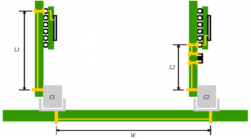
Typical backplane bus topology and layout between two daughterboards
In this setup, we need to use S-parameters from the following portions of the system:
- The left transmission line with length L1
- The central transmission line across the backplane with length W
- The left transmission line with length L1
- Both connectors C1 and C2
The S-parameter data from connectors C1 and C2 should be provided by the manufacturer or measured in-house. Here, we want to look at the S-parameters of the overall channel to see if insertion loss (S21) and return loss (S11) for the entire interconnect are within signal specs at the receiver component. This requires looking at the S-parameters and transfer function for the entire bus as a cascaded network.
Backplane Bus S-parameters
Unfortunately, S-parameter matrices cannot simply be multiplied together to produce S-parameters for a cascaded network except in specific situations. In general, you need to use some algorithm to determine the S-parameters for the cascaded backplane bus network.
Convert to ABCD Parameters by Hand
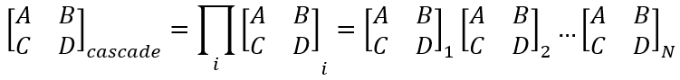
This is by far the simplest and yet most powerful way to get the S-parameters for your cascaded network. Simply calculate the ABCD-parameters for each portion of the system, multiply these ABCD matrices together, and convert the result back to S-parameters. ABCD-parameters (defined for LTI systems) can be cascaded through simple multiplication:
The formulas for converting between S-parameters and ABCD-parameters are well-known and can be found in many resources online. To summarize:
- Calculate the ABCD-parameters for each element in the simulation using each element's S-parameters
- Multiply the ABCD-parameters together to get the network's cascaded ABCD matrix
- Convert the cascaded ABCD matrix to get the S-parameter matrix for the network
Note that this is only useful when you have analytical expressions for the S-parameters as functions of frequency, or you are working at a single frequency. Otherwise, you must use a numerical algorithm.
Use MATLAB or a Similar Program
MATLAB has a built-in cascadesparams function that lets you input multiple S-parameter matrices, and it will calculate the cascaded matrix with the following syntax:
s_params= cascadesparams(s1_params,s2_params,...,sk_params)
Take a look at their documentation for more information. This tool lets you input numerical data for broadband S-parameters as functions for frequency. Note that this technique already uses a numerical conversion to ABCD parameters to get broadband S-parameters.
Use Signal Simulations in Your PCB Layout Tools
You could avoid the use of S-parameters altogether and simply use field solver-based utilities in your PCB layout software. Since backplane bus and connector arrangements are multi-board systems, not all PCB layout utilities can be used to simulate the entire system simultaneously. Instead, you need to look at signal transfer across each daughterboard and the backplane bus individually. Whether looking at the total system or individual parts, integrated simulation tools will show you signal responses without the need to extract S-parameters. This is normally performed by extracting S-parameters using the boundary element method (BEM) or method of moments (MoM) along the interconnect, followed by calculating a channel response for an input signal.
The Takeaway
The important point here is that individual transmission lines on the daughterboards and the backplane bus can't be considered individually in a backplane bus simulation if you want to accurately examine signal integrity. You need to treat all traces plus connectors as a cascaded network and simulate signal behavior within the entire network. In the event the signal at the receiver does not meet specs, you may want to simulate signal transfer between each element using ABCD parameters. The solution can be as simple as using a lower-loss substrate or slightly modifying the geometry in the transmission line; I'll discuss this last point in an upcoming article.
Here, we haven't considered vias along the backplane bus. Note that vias will have their own S-parameters and should be included in your network simulation for the backplane bus. As long as vias are short and backdrilled, you will have minimal signal integrity problems when vias are sized properly and the number of vias on an interconnect is minimized. Still, S-parameters for vias need to be included in the interconnect model as they can create some return loss along the interconnect. This is still a subject of active research for broadband digital/mixed-signal design and highly accurate modeling techniques are still being developed.
Once you get to the point where you have S-parameters for your system, you can simulate the impulse response in your backplane bus. You can then see if there will be transient ringing in the signal and the level of distortion in the time domain. Backplane design and simulation can be complicated, but the routing tools and xSignals package in Altium Designer can help expedite the design process for any backplane bus. These tools and many more are all accessible within a single program.
Contact us or download a free trial if you’re interested in learning more about Altium Designer®. You’ll have access to the industry’s best layout, simulation, and data management tools in a single program. Talk to an Altium expert today to learn more.
