How to Use Your CAD Tools for RF Trace Taper Design
PCB traces in RF systems must be designed to have specific impedance, which is normally 50 Ohms in order to limit reflection when interfacing with other RF components like antennas. Waveguide routing is often used and requires controlled impedance, but not all components can support wide traces used in RF waveguide routing. To provide the required interface with components, the end of an RF waveguide, including coplanar waveguide routing, can be tapered to connect to a component.
We’ve compiled a short guide on using your CAD tools to design a trace taper on RF traces. The best set of automated routing tools can help enforce the geometry you need to ensure consistent characteristic impedance and trace width.
ALTIUM DESIGNER
A unified PCB design application with a full suite of layout and manufacturing tools for professional RF PCB designers.
PCB design and routing transmission lines with high frequency RF signals can be challenging, but the best set of design tools can help automate your transmission line design process. It helps to understand the effect of a trace taper on RF interconnects as tapered traces are sometimes needed to connect to land patterns. In addition, tapering is used to connect to some RF components like an antenna or a new waveguide with alternative structure.
What is RF Trace Tapering?
A tapered trace in an RF interconnect is a length of a trace or waveguide that narrows into a component to make the required electrical connection. The frequency response, impedance, and the width of the taper need to be carefully designed so that there is minimized impedance mismatch at the connected components. If the RF waveguide taper width and length are set to the correct size, the input impedance of the waveguide will closely match the characteristic impedance of the waveguide.
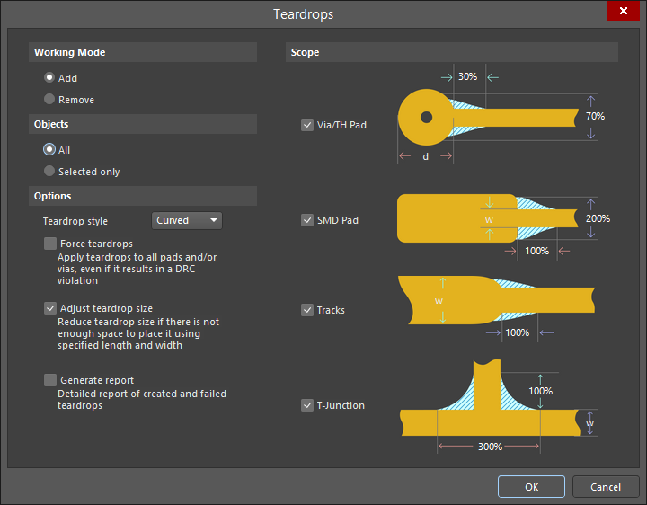
Your PCB design tools will use a feature called “teardrops” to apply tapers to traces, including RF trace tapers. These features can also be applied to vias, as shown below.

RF trace taper and teardrop on a via
When to Use Tapered RF Traces
RF trace tapers can be used in a few different situations:
- Impedance mismatch elimination: An RF trace taper can be used to ensure impedance matching between two different types of transmission lines or waveguides.
- Connecting to land patterns: Sometimes, a land is smaller than the width of your RF trace, so you’ll need to taper the width to make the connection to your component.
- Connecting to vias: Connecting to a via with a trace taper helps ensure conformance to IPC Class 3 reliability requirements.
- Connect to an antenna: Some antennas with unique geometry have thin or large feedline points, and the RF trace needs to have a taper applied to make the required connection.
With the design tools in Altium Designer, you can easily place and route trace tapers using the Teardrops feature, as shown in the image below. These features can be applied automatically to specific nets, or to all nets in a PCB layout.
- The best set of CAD tools and routing features can help you easily design and route a microstrip to waveguide transition.
Learn more about designing an RF microstrip to waveguide transition.
- Your PCB stackup also needs to be designed to ensure impedance controlled routing with standard transmission line geometries, including coplanar waveguide routing.
Learn more about PCB stackup design in your RF circuit board.
- Altium Designer makes RF layout and routing when working at any frequency thanks to its rules-driven design environment.
See an example project with RF routing created in Altium Designer.

Altium Designer’s teardrop features let you customize trace tapers, via tapers, and T-junction tapers.
RF Trace Tapering and Signal Impedance
RF waveguide traces need to be routed above a ground plane, which along with the dielectric constant of the PCB substrate will determine the characteristic impedance of the waveguide. For coplanar waveguide routing, the distance to the top-layer copper pour and grounded via fence along the feedline trace will also determine the characteristic impedance of the waveguide structure. Together with the location of the ground plane and the geometry of the RF trace, the taper will determine the input impedance of the trace s seen by a driving component.
Because the ground plane and the geometry of the RF trace are so important, designers need tools to help them quickly calculate impedance for their RF traces. These rules then need to applied to your routing to ensure your traces always have the right impedance.
How to Calculate the Taper Width for an RF Trace
There are some references that show how to design a taper for an RF trace, but these references use approximate formulas to ensure the input impedance of the trace matches the value for the driver/receiver/input impedances. The best PCB design tools will include a numerical electromagnetic field solver that can determine the best trace taper width for a desired characteristic impedance. This is by far the fastest way to determine the best trace taper width for your design while ensuring your routing complies with important RF PCB design rules.
- Altium Designer’s routing tools automatically apply the geometry you’ve set for your trace width and taper width as you route your PCB.
Learn more about Altium Designer’s interactive controlled impedance routing utilities.
- The best design tools can help you create unique waveguide architectures for RF signals, like substrate integrated waveguides.
- Once your design gets to ultra-high frequencies, you need to use an alternative to traditional waveguides with low loss, like a mode-selective transmission line.

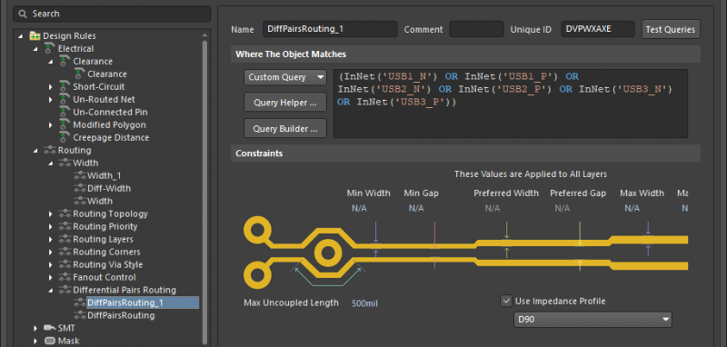
Altium Designer’s rules-driven design environment lets you apply impedance profiles to your RF interconnects.
Everything You Need for RF PCB Design
Successful creation of RF PCBs takes more than just tapered traces. Designers need schematic design and capture features that instantly drop components into their PCB layouts. Designers also need documentation tools that automatically generate PCB manufacturing deliverables directly from PCB layout data. Altium Designer includes all this and much more, and all these features are present in a single design application.
Altium Designer Helps You Create Electronics With Maximum Productivity
The rules-driven design engine in Altium Designer unifies every design tool you need into a single application. Everything needed for design, layout, component sourcing, and manufacturing can be found in Altium Designer’s unified environment. You can stay productive and ensure ultra-accurate assembly with Altium Designer.
- Altium Designer includes everything needed to design simple circuit boards and advanced high frequency PCBs in a single application.
Learn more about Altium Designer’s unified design environment.
- Altium Designer now includes an integrated field solver from Simberian, giving designers an integrated tool for ultra-accurate impedance calculations.
Learn more about the integrated field solver from Simberian in Altium Designer.
- When you’re ready to share your circuit board with other PCB designers or your manufacturer, Altium 365 lets you instantly share your design and production data through Altium Designer or on the web.
Learn more about sharing your PCB project data with Altium 365.

Altium Designer provides everything needed for high speed PCB design and RF PCB design ina single application.
Designing an RF trace taper shouldn’t take a commercial field solver application. Altium Designer gives you the tools you need to apply RF trace tapers and verify routing and impedance against your design rules. You can stay productive while designing high frequency systems and preparing for manufacturing when you use Altium Designer.
Altium Designer on Altium 365 delivers unprecedented integration to the electronics industry until now relegated to the world of software development, allowing designers to work from home and reach unprecedented levels of efficiency.
We have only scratched the surface of what is possible to do with Altium Designer on Altium 365. You can check theproduct page for a more in-depth feature description or one of theOn-Demand Webinars.
