Prepare to Share: How to Make the Most of Collaborative PCB Design

If you have experience working on PCB design teams, either in a single location or remotely, you’ve probably seen your share of successful and failed projects. Any project can fail or be severely delayed for a variety of reasons, and sometimes the stars must align to ensure everything is delivered on-time and under-budget. Even after making many mistakes that caused project delays and fragmented team members, I’m still learning what it takes to make sure every project is successful.
After learning from my blunders as a project manager, there are a few things I try to do before I start sharing client data with my design team. For newer recent projects, and even in the middle of ongoing projects, I’ll try to go through these tasks to make sure we avoid a redesign before delivering final design data. Make sure to check these points (and I’m sure many others) before you send project requirements, tasks, and design data out to team members.
What to Check Before You Share
Getting complete functional and DFM requirements before starting a layout are important tasks, but there is more that needs to be done before sharing design data. The goal in these tasks is to prevent unnecessary design changes once the layout nears completion. Here are some points that have popped up repeatedly in my projects:
Sanitize Your BOM
I’ve had this experience multiple times when taking on a new project: the customer sends 6-month old schematics, libraries, and a BOM. Once the new project is created to get the layout started, you suddenly find half the components have gone EOL, LTB, NRND, obsolete, or out of stock. Nowadays, I make sure to sanitize the BOM on the front-end by just placing the schematic and libraries into a new project, then I create a new BOM and count up the number of components with problems. I always want to make sure my clients know what other tasks are involved in getting their design ready for layout and manufacturing, and sanitizing a BOM is one of those important tasks.
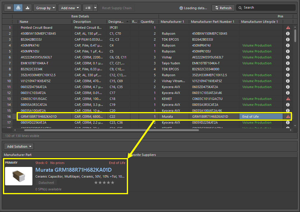
This task of cleaning up a BOM can take days for larger problem-ridden projects, but it always prevents wasted time later. If you do this before starting the layout, you won’t have to risk more extensive redesigns once you’re ready to start fabrication and assembly. It helps when you have access to supply chain data inside your bill of materials as this cuts down on time spent scanning distributor websites.
Get a Clear List of Planned Changes from the Client
Have you ever had a client come to you with updated mechanical or component changes right as you’re about to finish their PCB layout? I’ve had this happen before, and it can be infuriating. In some cases, it’s just a matter of resizing mounting holes or shifting a couple components. Other times, it can force extensive redesigns, and you start to wish someone would have mentioned it before you started the layout.
In a recent project, a simple request to move 6 SMA connectors down by ~0.5 cm forced us to move all other connectors on the bottom half of the board. This also required a decent amount of rerouting and repouring polygons on multiple layers. If we had gotten word of these changes earlier, we could have saved our time and the client’s money. Getting these changes ahead of time allows the layout team to plan for them by saving component placement and routing in these areas until last.
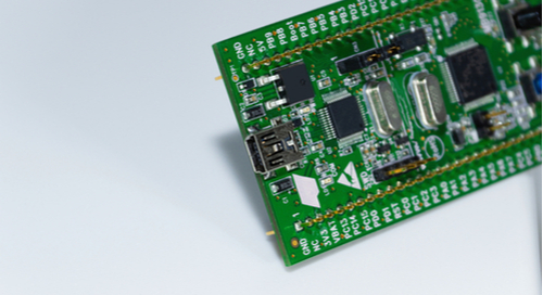
For Embedded: Get Your Dev Boards and Start Coding Early!
Myself and my designers all swear by dev boards for speeding up embedded development. This is one of those tasks that can be performed in parallel if you have the staff to support it. You also don’t need to have a layout or schematics finished before you start putting code together; you only need to have a high-level block diagram and some functional requirements.
We do this whenever we have an embedded project with an MCU/FPGA that needs to interface with other ICs. Any problems that require debugging during development are already narrowed down to the code-level and should have nothing to do with the dev board layout. It never hurts to do a Google search for dev boards and get a list over to your firmware engineer; you might be surprised at the range of available dev boards.
Can Tasks Run in Parallel?
This is one aspect of project management that is obvious in hindsight, but it is something I was still learning to anticipate in some of my first projects. If you obtained thorough requirements and planned design changes before you share project data and assign tasks, you can spot which tasks might best be run in parallel. During the design phase. Multi-board layouts, coding for any embedded firmware, and any software apps that need to interface with the system are all candidate tasks that could run in parallel.
Agree on Times to Discuss Progress
This is another point that seems simple, but it makes all the difference for getting tough questions answered early as your team works through a design. Regular check-in times (be they daily or weekly) give everyone an opportunity to share progress, resolve outstanding questions, and set action items.
Ready to Share? Use Altium 365
Whether everyone is collaborating remotely or is clustered in an office, get these up-front tasks done before you start working on the design. When you’re ready to share your design data and begin a project, the management and sharing features on Altium 365® will help keep everyone on the same page. These features are accessible within Altium Designer®, giving everyone on your team a complete tool for collaborative PCB design.
When you use Altium Designer on the Altium 365 platform, you can create a productive and collaborative PCB design workflow for your team. Altium 365 lets you bring designers, end users, and manufacturers into the development process, which can help you get through a design review faster and avoid time-consuming redesigns. Everyone on your team will have access to supply chain data, commenting features, and data sharing tools to help streamline PCB design collaboration.
We have only scratched the surface of what is possible to do with Altium Designer on Altium 365. You can check the product page for a more in-depth feature description or one of the On-Demand Webinars.
